Method for improving thickness uniformity of single crystal piezoelectric film

A piezoelectric film with uniform thickness, applied in piezoelectric/electrostrictive/magnetostrictive devices, circuits, electrical components, etc. question

Active Publication Date: 2020-10-27
SHANGHAI NOVEL SI INTEGRATION TECH CO LTD
View PDF4 Cites 1 Cited by
  • Summary
  • Abstract
  • Description
  • Claims
  • Application Information

AI Technical Summary

Problems solved by technology

[0004] However, in the process of preparing single-crystal piezoelectric thin films using ion beam exfoliation technology, since piezoelectric materials usually have a large thermal expansion coefficient, the piezoelectric material and the support substrate have a large thermal expansion coefficient mismatch. There will be a large thermal stress. Compared with silicon-on-insulator, this thermal stress will affect the aggregation and stripping of implanted ions, which will cause great inhomogeneity in the transferred target single-crystal piezoelectric film, while Larger thickness inhomogeneity, that is, a larger deviation from the expected film thickness, will directly affect the yield of related acoustic devices, electrical devices, and optical devices using the transferred piezoelectric film, and thus appear due to the Unusable problems due to uneven thickness

Method used


Image

  • Method for improving thickness uniformity of single crystal piezoelectric film
  • Method for improving thickness uniformity of single crystal piezoelectric film
  • Method for improving thickness uniformity of single crystal piezoelectric film

Examples


Embodiment

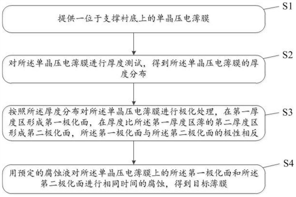
[0039] This embodiment provides a method for improving the uniformity of the thickness of a single crystal piezoelectric film, see figure 1 , the method for improving the uniformity of the thickness of the single crystal piezoelectric thin film of the present embodiment comprises the following steps:

[0040] Step S1, providing a single crystal piezoelectric thin film on a supporting substrate.

[0041] In this embodiment, ion implantation is performed on the piezoelectric single crystal substrate by ion beam stripping technology, and the implanted material is bound to the supporting substrate material by bonding technology, and the aggregation of ions in the material is realized by means of heating The purpose of transferring the target single crystal piezoelectric film is achieved. High-quality single-crystal thin films can be integrated on amorphous, polycrystalline, and even flexible substrates by ion beam exfoliation, providing a simple and efficient means for realizing ...


PUM

PropertyMeasurementUnit
thicknessaaaaaaaaaa
thicknessaaaaaaaaaa

Abstract

The invention discloses a method for improving the thickness uniformity of a single crystal piezoelectric film, and belongs to the technical field of semiconductor manufacturing. According to the method for improving the thickness uniformity of the single crystal piezoelectric film, polarization processing is carried out according to the thickness distribution of the single crystal piezoelectric film on a support substrate, a first polarization surface is formed in a first thickness region, a second polarization surface is formed in a second thickness region which is thinner than the first thickness region, and the polarities of the first polarization surface and the second polarization surface are opposite. The anisotropic characteristic of the piezoelectric single crystal material is utilized, under the same corrosive liquid, the first polarization surface obtained through polarization of a thicker area is corroded at a high speed, and the second polarization surface obtained throughpolarization of a thinner area is corroded at a low speed, so that differential corrosion of different polarization surfaces of the single crystal piezoelectric film is achieved. Compared with the prior art, the method has the advantages that the thickness uniformity of the single crystal piezoelectric film can be optimized, and the thickness uniformity of the single crystal piezoelectric film isgreatly improved.

Description

technical field [0001] The invention relates to the technical field of semiconductor manufacturing, in particular to a method for improving the thickness uniformity of a single crystal piezoelectric film. Background technique [0002] Ion beam lift-off technology is a combination of bonding technology and ion implantation. By implanting ions in the material, the implanted material is bound to the support material by bonding technology, and the ions are gathered in the material under heating and other methods to achieve Transfer of a thin film of injected material. [0003] At present, ion beam exfoliation technology, as a commonly used material heterogeneous integration method, can prepare high-quality single crystal thin films with uniform and controllable thickness, and has been widely used in the preparation of silicon-on-insulator. Due to the great flexibility of the ion beam stripping technology, it can avoid the difference between the crystal form, lattice constant an...

Claims


Application Information

Patent Timeline
Patent Type & Authority Applications(China)
IPC IPC(8): H01L41/257H01L41/332H01L21/66
CPCH01L22/12H10N30/045H10N30/082
Inventor 欧欣李忠旭黄凯赵晓蒙李文琴鄢有泉陈阳
Owner SHANGHAI NOVEL SI INTEGRATION TECH CO LTD
Why Eureka
Try Eureka