Photodetector and method of making the same

A technology of a photodetector and a manufacturing method, applied in the field of photodetection, can solve the problems of poor focusing effect, complex device process and high cost, and achieve the effects of reducing device process difficulty, improving coupling efficiency and reducing cost

Active Publication Date: 2022-05-13
UNIV OF SCI & TECH OF CHINA
View PDF4 Cites 0 Cited by
  • Summary
  • Abstract
  • Description
  • Claims
  • Application Information

AI Technical Summary

Problems solved by technology

[0003] For PIN-type photodetectors, in order to couple light from the waveguide to the absorbing layer, evanescent wave-coupled waveguide-type PIN photodetectors usually use a refractive index between InP and In 0.53 Ga 0.47 The quaternary InGaAsP material with As refractive index is used as the optical matching layer. In the prior art, one optical matching layer and two optical matching layers are used. The focusing effect is poor, the device process is complicated, and the cost is high.

Method used


Image

  • Photodetector and method of making the same
  • Photodetector and method of making the same
  • Photodetector and method of making the same

Examples


Embodiment Construction

[0058]The following will clearly and completely describe the embodiments of the present invention with reference to the accompanying drawings in the embodiments of the present invention. Apparently, the described embodiments are only some, not all, embodiments of the present invention. Based on the embodiments of the present invention, all other embodiments obtained by persons of ordinary skill in the art without making creative efforts belong to the protection scope of the present invention.

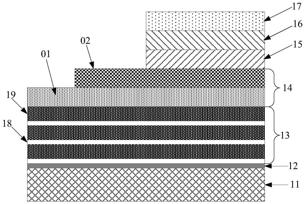
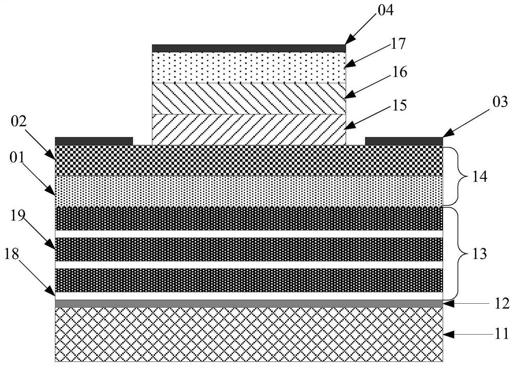
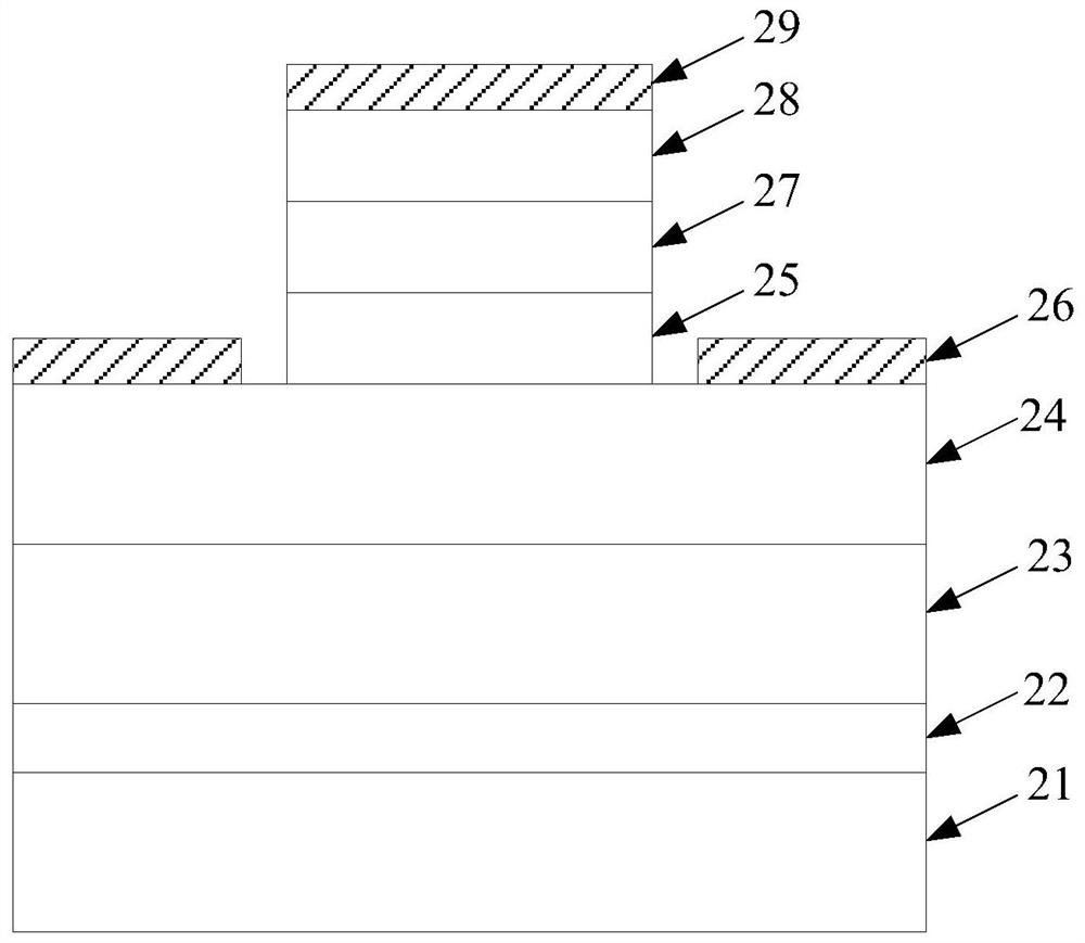
[0059] Optical communication technology is developing in the direction of high speed and large capacity. The photoelectric converter at the receiving end converts optical signals into high-frequency electrical signals. High-speed photodetectors with high quantum efficiency and high power processing capabilities are the key components. For the 1310nm and 1550nm bands of the optical fiber communication window, the III-V group direct bandgap semiconductor material InP, and its lattice-match...


PUM

PropertyMeasurementUnit
thicknessaaaaaaaaaa
lengthaaaaaaaaaa
thicknessaaaaaaaaaa

Abstract

The invention discloses a photodetector and a manufacturing method thereof. The photodetector comprises: a substrate; a buffer layer arranged on the substrate; a waveguide arranged on the side of the buffer layer away from the substrate layer; a graded optical matching layer arranged on the side of the waveguide layer away from the buffer layer; an absorbing layer and a cathode arranged on the side of the graded optical matching layer away from the waveguide layer; arranged on the absorbing layer away from the buffer layer The cladding layer on one side of the graded optical matching layer; the contact layer arranged on the side of the cladding layer away from the absorption layer; the anode arranged on the side of the contact layer; wherein, the graded optical matching layer is a single layer In a thin film, in a first direction, the refractive index of the graded optical matching layer gradually increases; the first direction is directed from the waveguide layer to the absorption layer. By applying the technical scheme provided by the invention, focusing in advance can be realized, coupling efficiency can be improved, device process difficulty can be reduced, and cost can be reduced.

Description

technical field [0001] The invention relates to the technical field of photoelectric detection, and more specifically, to a photoelectric detector and a manufacturing method thereof. Background technique [0002] Photodetectors are one of the key devices in the field of semiconductor optoelectronic devices, and have been widely used in optical communications, optical sensing, optical imaging, and autonomous driving in recent years. Especially in applications such as optical sensing and long-distance imaging, not only photodetectors are required to have high responsivity and high speed, but also devices are required to have a wide spectral range. [0003] For PIN-type photodetectors, in order to couple light from the waveguide to the absorbing layer, evanescent wave-coupled waveguide-type PIN photodetectors usually use a refractive index between InP and In 0.53 Ga 0.47 The quaternary InGaAsP material with As refractive index is used as the optical matching layer. In the pri...

Claims


Application Information

Patent Timeline
Patent Type & Authority Patents(China)
IPC IPC(8): H01L31/0232H01L31/0216H01L31/105H01L31/18
CPCH01L31/105H01L31/1844H01L31/02327H01L31/02161Y02P70/50
Inventor 张博健王亮王方莉郭松坡
Owner UNIV OF SCI & TECH OF CHINA
Why Eureka
Try Eureka