Preparation method of solder micro-bump array

A technology of solder bumps and micro-bumps, which is applied in semiconductor/solid-state device manufacturing, electrical components, electrical solid-state devices, etc. simple effect

Active Publication Date: 2020-11-03
CHINA ELECTRONIC TECH GRP CORP NO 38 RES INST
View PDF8 Cites 2 Cited by
  • Summary
  • Abstract
  • Description
  • Claims
  • Application Information

AI Technical Summary

Problems solved by technology

[0005] The technical problem to be solved by the present invention is: the technical problems of the solder micro-bump preparation method in the prior art with complex process, low efficiency and high cost

Method used


Image

  • Preparation method of solder micro-bump array

Examples


Embodiment 1

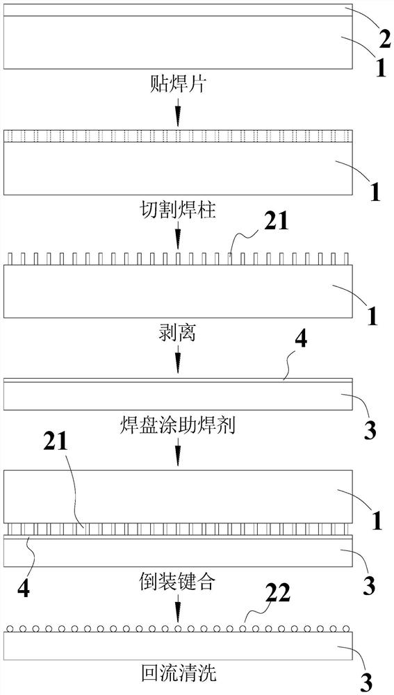
[0038] A method for preparing a solder micro-bump array, comprising the steps of:

[0039] Before step s1, the raw materials need to be processed, that is, the required model and thickness of the solder sheet 2 should be prepared, cut to the required size, to ensure that the solder sheet is flat, and if necessary, it can be leveled to prepare the required Carrier plate 1 of shape and size, cleaning the surface.

[0040] s1. Paste solder tabs:

[0041] Such as figure 1 As shown, attach the solder piece 2 to the carrier board 1; specifically, apply the adhesive on the clean carrier board 1, spread the glue fully and evenly by high-speed spinning or scraping, and place the flat solder piece 2 Attached to carrier board 1.

[0042] Solder piece 2 adopts commonly used Sn-based, Pb-based, In-based, AuSn solder pieces, such as Sn 50 In 50 , Sn 43 Pb 43 Bi 14 , Sn 62 Pb 36 Ag 2 , Sn 63 Pb 37 , SAC305, Sn 90 Sb 10 , Pb 90 sn 10 、Au 80 sn 20 Wait. According to the siz...

Embodiment 2

[0060] s1. Paste solder tabs:

[0061] Apply 502 glue adhesive on the clean glass carrier, spread the glue fully and evenly by spinning the glue at a high speed, the speed is 2000rpm, and the time is 30s. The thickness of the formed glue is 30-50μm, and the leveled Pb with a thickness of 100μm 63 sn 37 The solder tabs are attached to the glass carrier.

[0062] s2. Cutting:

[0063] Cut out a 10*10 array of solder columns on the solder sheet according to the design pattern with a UV laser processing equipment with a laser power of 10W. The laser power is set to 70%, the frequency is 35KHz, the marking speed is 300mm / s, and the diameter of the processed solder column is 100μm .

[0064] s3, stripping:

[0065] Use tweezers to tear off the excess solder sheet as a whole, leaving only the array of solder posts, and inspect the array of solder posts under a microscope.

[0066] s4. Flip-chip welding:

[0067] Brush a layer of flux on the surface of the chip pad, and use a f...


PUM

PropertyMeasurementUnit
thicknessaaaaaaaaaa

Abstract

The invention relates to the field of chip packaging, in particular to a preparation method of a solder micro-bump array, and the method comprises the following steps: pasting of a soldering lug: pasting the soldering lug on a carrier plate; cutting: cutting out a solder column array on the soldering lug; peeling: tearing off or peeling off the redundant soldering lugs, and only leaving the soldercolumn array; flip-chip bonding: transferring the solder column array to a bonding pad needing to be provided with a salient point area array. and reflowing: reflowing the bonding pad with the soldercolumn array to melt the solder column array into a ball so as to form a regular solder bump array. The method has the advantages that the method is simple in process, high in efficiency, flexible, convenient, suitable for welding flux of various types, free of specially-made microspheres, low in cost, suitable for overall manufacturing of wafers and suitable for cut chips and adapter plates, a specially-made ball mounting template is not needed, and large-scale application can be achieved.

Description

technical field [0001] The invention relates to the field of chip packaging, in particular to a method for preparing a solder microbump array. Background technique [0002] In order to meet the requirements of miniaturization and high integration of electronic components, sub-systems and complete machines in the future, it is urgent to develop combination technologies of flip chip, stacked chip or device, embedded device or multilayer packaging to achieve high assembly density and function density. Advanced assembly technologies such as flip-chip and chip stacking mostly use the area array bump interconnection process, which has the advantages of saving area, reducing lead length, facilitating heat dissipation, improving performance and reducing volume, and is a highly competitive technology. and development potential of packaging technology. Therefore, in order to develop advanced assembly technology for microsystems, it is first necessary to realize interconnected area a...

Claims


Application Information

Patent Timeline
Patent Type & Authority Applications(China)
IPC IPC(8): H01L23/488H01L21/48H01L21/60
CPCH01L23/488H01L21/4814H01L24/11H01L24/14
Inventor 刘建军胡海霖郭育华张孔王运龙
Owner CHINA ELECTRONIC TECH GRP CORP NO 38 RES INST
Why Eureka
Try Eureka