Electrostatic protection GGNMOS structure

An electrostatic protection, N-type technology, used in circuits, electrical components, electrical solid devices, etc., can solve the problems of weak ESD capability and small PN junction contact area, and achieve the effect of enhancing ESD capability

Pending Publication Date: 2020-11-03
SHANGHAI HUAHONG GRACE SEMICON MFG CORP
View PDF0 Cites 3 Cited by
  • Summary
  • Abstract
  • Description
  • Claims
  • Application Information

AI Technical Summary

Problems solved by technology

like image 3 and Figure 4 As shown, the body diode formed in this way has ver

Method used


Image

  • Electrostatic protection GGNMOS structure
  • Electrostatic protection GGNMOS structure
  • Electrostatic protection GGNMOS structure

Examples


Embodiment Construction

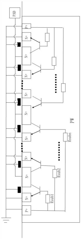
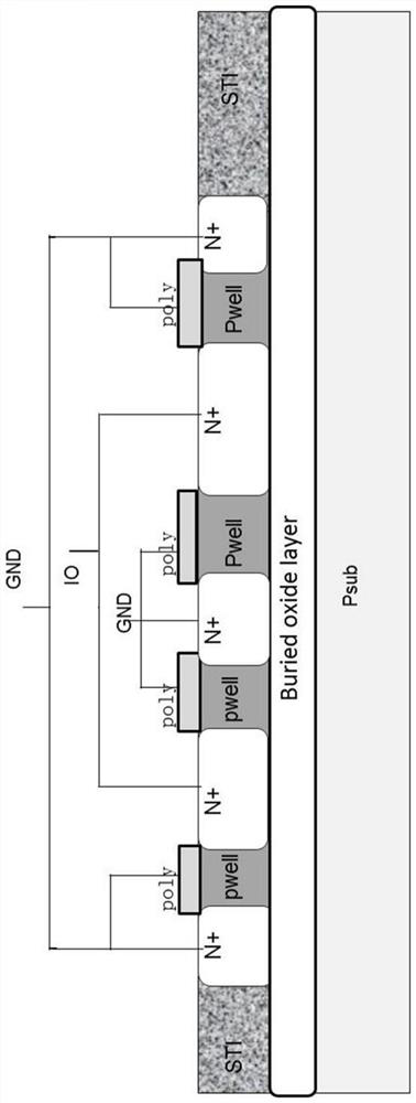
[0026] The electrostatic protection GGNMOS structure described in the present invention is based on the finger-shaped GGNMOS device of the SOI process, and its cross-sectional structure can be specifically referred to as Figure 5 Sectional view and combination of Figure 6 As shown in the planar layout, the embodiment of the present invention mainly takes NMOS as an example, that is, GGNMOS. For PMOS, that is, GDPMOS, the doping type of the relevant structure can be reversed. This embodiment only uses the GGNMOS structure for the following description.

[0027] For GGNMOS, a buried oxide layer (Buried oxide layer) is formed in a P-type substrate by SOI process.

[0028] In the upper layer of the substrate, that is, above the buried oxide layer, an active area is defined by the STI process, and a plurality of P wells are formed in the active area, and the plurality of P wells are spaced apart from each other.

[0029] There is a heavily doped N-type implant region between the...


PUM


Abstract

The invention discloses an electrostatic protection GGNMOS structure, which is suitable for an interdigital GGNMOS of an SOI process. In the upper layer of the substrate, an active region is defined through an STI process, a plurality of P wells are formed in the active region, and the plurality of P wells are mutually spaced; a heavily doped N-type injection region is arranged between the P trapand the peripheral STI; heavily doped N-type injection regions are arranged between the P wells at intervals; the heavily doped N-type injection region is in transverse contact with the P trap; and aheavily doped P-type injection region is arranged between the P wells in the central region, and the heavily doped P-type injection region is in transverse contact with the P wells on the two sides ofthe heavily doped P-type injection region. According to the invention, through the P trap and the heavily doped P-type injection region in the central region, each insertion finger forms a body diodefrom S/B to the drain end, so that the ESD capability of the GGNMOS in the direction of the body diode is enhanced.

Description

technical field [0001] The invention relates to the field of design and manufacture of semiconductor devices, in particular to an electrostatic protection GGNMOS structure based on SOI technology. Background technique [0002] Static electricity is an objective natural phenomenon, which can be produced in many ways, such as contact, friction, induction between electrical appliances, etc. Static electricity is characterized by long-term accumulation, high voltage, low power, small current and short action time. Static electricity causes serious harm in many fields. Friction electrification and human body static electricity are two major hazards in the electronics industry, which often cause unstable operation or even damage of electronic and electrical products. [0003] As the feature size of the semiconductor integrated circuit manufacturing process becomes smaller and smaller, the size of the chip unit is also smaller and smaller, and the antistatic ability of the chip b...

Claims


Application Information

Patent Timeline
IPC IPC(8): H01L27/02H01L27/12H01L29/78
CPCH01L27/0255H01L27/0207H01L27/1203H01L29/78
Inventor 邓樟鹏
Owner SHANGHAI HUAHONG GRACE SEMICON MFG CORP
Why Eureka
Try Eureka