Semiconductor forming method and structure thereof

A semiconductor and graphics technology, applied in the direction of semiconductor devices, semiconductor/solid-state device manufacturing, semiconductor/solid-state device components, etc., can solve the problems of low utilization efficiency of a single wafer, small number of effective chips, etc., to improve area utilization , Improve the effect of alignment accuracy

Active Publication Date: 2020-11-10
SEMICON MFG INT (SHANGHAI) CORP +1
View PDF9 Cites 1 Cited by
  • Summary
  • Abstract
  • Description
  • Claims
  • Application Information

AI Technical Summary

Problems solved by technology

[0006] The problem solved by the present invention is that the utilization efficiency of the existing single wafer is low, and the number of effective chips is small

Method used


Image

  • Semiconductor forming method and structure thereof
  • Semiconductor forming method and structure thereof
  • Semiconductor forming method and structure thereof

Examples


no. 1 example

[0031] Figure 1 to Figure 5 is a schematic diagram of an alignment mark forming method provided by an embodiment of the present invention.

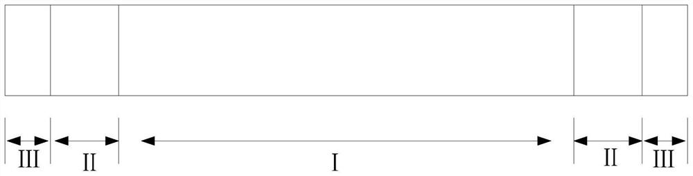
[0032] refer to figure 1 , provide a chip, the chip includes a chip device area I, a dummy device area II on the periphery of the chip device area I, the periphery of the dummy device area II also includes a sealing device area III, and a dicing line ( not shown).

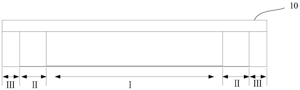
[0033] refer to figure 2 , forming a photoresist layer 10 on the surface of the dummy device region II. Specifically, the method for forming the photoresist layer 10 is a dynamic spray coating method, which first rotates at a low speed so that the photoresist is uniformly diffused, and then rotates at a high speed to form a uniform photoresist in the dummy device region II. Resist layer 10.

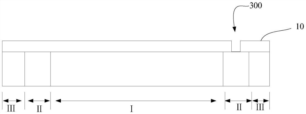
[0034] refer to image 3 , transferring the pattern with the alignment mark 300 of the present invention onto the photoresist layer 10 . The specific steps include: placing a mas...

no. 2 example

[0054] Figure 8 It is a schematic diagram of the pattern of the alignment mark provided by another embodiment of the present invention.

[0055] refer to Figure 8 , in this embodiment, the alignment mark 300 is Figure 6 The structure of the alignment mark in is effectively split, and can be formed in the dummy device region II without affecting the function of the alignment mark 300 . Specifically, the alignment mark 300 includes a first alignment mark aligned in a first direction x and a second alignment mark aligned in a second direction y, and the first alignment mark is aligned with the second alignment mark. The quasi-identification is separated. The purpose of splitting the alignment mark 300 is to ensure that the alignment mark 300 is completely formed in the dummy device region II due to the limited area size of the dummy device region II.

[0056] In this embodiment, the first alignment mark includes the grating group A and the grating group D. It can be seen t...


PUM

PropertyMeasurementUnit
Spacingaaaaaaaaaa
Lengthaaaaaaaaaa
Widthaaaaaaaaaa

Abstract

The invention discloses a semiconductor forming method and a structure thereof, and the forming method comprises the steps of providing a chip which is provided with a virtual device region; and forming an alignment mark in the virtual device region. The alignment mark is separated from other alignment patterns in an original cutting channel, the alignment requirement is met, but also an exposuredevice can identify the alignment mark more easily, the interference between optical interferometers is reduced, and the resolution is improved, so that the alignment precision can be improved. On theother hand, the virtual device region is effectively utilized, so that the area utilization rate of the wafer is improved.

Description

technical field [0001] The invention relates to the field of semiconductor manufacturing, in particular to a semiconductor forming method and its structure. Background technique [0002] In the field of semiconductors, with the improvement of critical dimension technology, the precision and process control of semiconductor processes have become more important. In the process of manufacturing semiconductor chips, the most important process is photolithography, which is the process of transferring mask patterns to wafers through a series of steps such as alignment, exposure, and etching; therefore, photolithography The engraving process directly affects the performance of the final chip structure. [0003] In the photolithography process, in order to transfer the mask pattern to the wafer correctly, the key step is to align the mask with the wafer, that is, to calculate the position of the mask relative to the wafer, so as to meet the requirements of overlay accuracy. When t...

Claims


Application Information

Patent Timeline
IPC IPC(8): H01L23/544H01L21/67G03F9/00
CPCH01L23/544H01L21/67282G03F9/7073H01L2223/54426
Inventor 熊鹏
Owner SEMICON MFG INT (SHANGHAI) CORP
Why Eureka
Try Eureka