Area array back incidence type solar blind ultraviolet detector and preparation method thereof
An ultraviolet detector and back-incidence technology, which is applied in the field of photodetectors, can solve the problems such as the inability to apply large-area arrays in the form of wire bonding packaging, increase the design difficulty and manufacturing cost, etc., so as to increase the effective incident area and improve the process reliability. , the effect of improving detection efficiency
- Summary
- Abstract
- Description
- Claims
- Application Information
AI Technical Summary
Problems solved by technology
Method used
Image

Examples
preparation example Construction
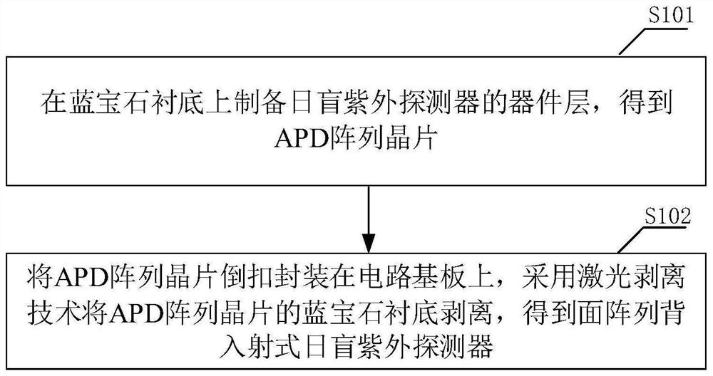
[0043] Please refer to figure 1 , figure 1 It is a schematic flow chart of the preparation method of the area array back-incidence solar-blind ultraviolet detector provided by an embodiment of the present invention. The preparation method of the surface array back-incidence solar-blind ultraviolet detector comprises:
[0044] S101: preparing a device layer of a solar-blind ultraviolet detector on a sapphire substrate to obtain an APD array wafer.
[0045] S102: The APD array chip is packaged upside down on the circuit substrate, and the sapphire substrate of the APD array chip is peeled off by laser lift-off technology to obtain a surface array back-incidence solar-blind ultraviolet detector.
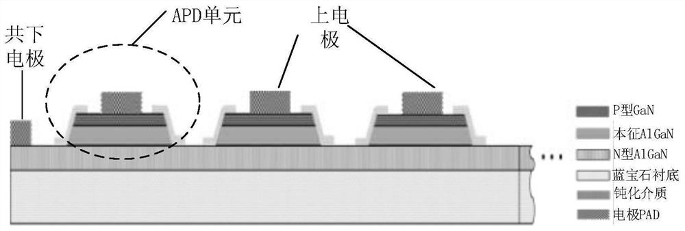
[0046] In this example, you can refer to Figure 2-Figure 5 The front side of the APD array chip is the side on which the electrodes are arranged, and the APD array chip is packaged upside down on the circuit substrate, even if the electrodes of the APD array chip are in contact with...
specific Embodiment approach
[0075] Optionally, as a specific implementation of the area array back-incidence solar-blind ultraviolet detector provided in the embodiment of the present invention, the APD array wafer includes:
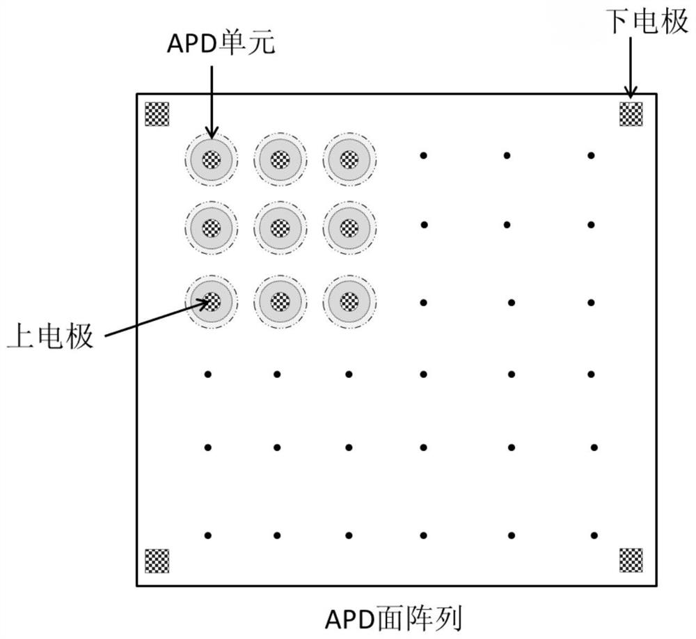
[0076] A sapphire substrate, an alignment mark located in a first predetermined area of the sapphire substrate, and a plurality of APD units located in a second predetermined area of the sapphire substrate.
[0077] The alignment mark is used to indicate the packaging position of the APD array chip, and a plurality of APD units are arranged at preset intervals.
[0078] Optionally, as a specific implementation of the area array back-incidence solar-blind ultraviolet detector provided in the embodiment of the present invention, the APD unit includes:
[0079] An N-type ohmic contact layer grown on a sapphire substrate.
[0080] A type I light absorbing layer grown on an N type ohmic contact layer.
[0081] A P-type ohmic contact layer grown on an I-type light absorbing layer. ...
PUM
 Abstract
Description
Claims
Application Information
 - R&D
- Intellectual Property
- Life Sciences
- Materials
- Tech Scout
- Unparalleled Data Quality
- Higher Quality Content
- 60% Fewer Hallucinations
Browse by: Latest US Patents, China's latest patents, Technical Efficacy Thesaurus, Application Domain, Technology Topic, Popular Technical Reports.
© 2025 PatSnap. All rights reserved.Legal|Privacy policy|Modern Slavery Act Transparency Statement|Sitemap|About US| Contact US: help@patsnap.com