
Semiconductor epitaxial wafer for 1550 nm wavelength laser

A technology of epitaxial wafers and lasers, which is applied to the structure of optical waveguide semiconductors, lasers, semiconductor lasers, etc., can solve problems such as large optical dispersion, low quality of outgoing light beams, reduced beam coherence and optical power density, etc., to achieve enhanced lateral constraints , Enhance the effect of beam quality

Active Publication Date: 2020-11-13
厦门中芯晶研半导体有限公司
View PDF1 Cites 0 Cited by
  • Summary
  • Abstract
  • Description
  • Claims
  • Application Information

AI Technical Summary

Problems solved by technology

[0005] Thirdly, the semiconductor laser mainly includes internal loss and cavity surface loss. The internal loss is mainly caused by the large optical dispersion caused by internal carrier absorption in the epitaxial material and waveguide scattering loss. Especially in the 1550nm optical band field, the p-layer The absorption of free carriers is quite high, resulting in a large optical loss; it will inevitably lead to a reduction in the optical power of the 1550nm band laser
Since the design of the waveguide region in the semiconductor epitaxial wafer cannot limit the lateral and lateral modes, the beam quality of the outgoing light is low, and the co-existence of multiple modes also reduces the coherence and optical power density of the beam.

Method used

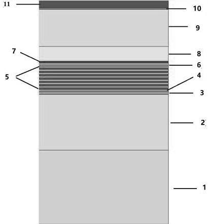
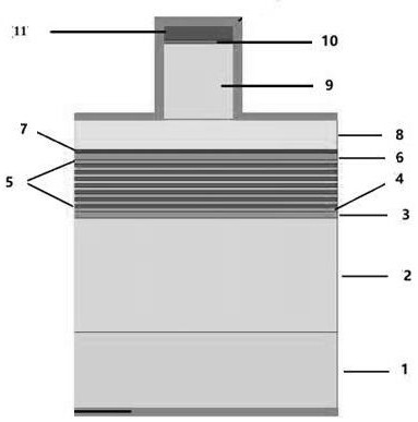

Image

  • Semiconductor epitaxial wafer for 1550 nm wavelength laser
  • Semiconductor epitaxial wafer for 1550 nm wavelength laser

Examples


Embodiment Construction

[0023] Preferred embodiments of the present invention will be described in detail below in conjunction with the accompanying drawings.

[0024] see figure 1 ,, a semiconductor epitaxial wafer for a 1550nm wavelength laser, comprising:

[0025] n-type InP substrate 1;

[0026] n-type InP capping layer 2, which is made on the substrate 1, and the thickness of the n-InP capping layer is 1000nm;

[0027] Non-doped Al x In y Ga (1-x-y) As confinement layer 3, which is made on the n-type cap layer, the thickness of the non-doped confinement layer is 60nm;

[0028] Non-doped Al x In y Ga (1-x-y) As barrier layer 4, which is made in non-doped Al x In y Ga (1-x-y) On As, the thickness of the non-doped barrier layer is 13nm;

[0029] al x In y Ga (1-x-y) As / Al x In y Ga (1-x-y)As strained quantum well structure 5, which is fabricated on the non-doped barrier layer, the Al x In y Ga (1-x-y) As / Al x In y Ga (1-x-y) As strained quantum well is an undoped strained qu...


PUM

PropertyMeasurementUnit
thicknessaaaaaaaaaa
thicknessaaaaaaaaaa
thicknessaaaaaaaaaa

Abstract

The invention discloses a semiconductor epitaxial wafer for a 1550nm wavelength laser. The semiconductor epitaxial wafer comprises an n-InP substrate, and a cover layer, a limiting layer, a barrier layer, a quantum well, a limiting layer, a protective layer, a diluted waveguide layer, a cover layer, a transition layer and an ohmic contact layer which are sequentially arranged on the substrate upwards. The semiconductor epitaxial wafer is divided into a substrate material, a passive waveguide region, an active region, a diluted waveguide region and a ridge waveguide, and the optical power of the semiconductor laser is improved by reducing absorption of a semiconductor epitaxial wafer with internal loss in a 1550nm wavelength laser photon cavity in a p-layer material. A ridge waveguide structure formed by the cover layer, the transition layer and the ohmic contact layer is used for increasing the transverse limitation of enhanced light in the semiconductor laser epitaxial structure and improving the light field distribution of a 1550nm-wavelength laser semiconductor epitaxial wafer.

Description

technical field [0001] The invention belongs to the field of semiconductors, and in particular relates to an epitaxial wafer for edge-emitting lasers with high power and high beam quality (near-field distribution, far-field distribution, divergence angle). Background technique [0002] Semiconductor lasers are widely used in communications, pumping sources of solid-state lasers and fiber lasers, laser printing, laser medical treatment, and space communications because of their small size, high reliability, long life, high conversion efficiency, simple drive, and direct modulation. and other fields. [0003] In the application of optical fiber communication and other fields, due to the need to directly couple the beam emitted by the edge-emitting laser into the single-mode fiber, the coupling efficiency of other modes other than the fundamental mode into the unidirectional fiber is very low. In order to overcome these problems, enhanced The design of semiconductor epitaxial ...

Claims


Application Information

Patent Timeline
Patent Type & Authority Applications(China)
IPC IPC(8): H01S5/20H01S5/22
CPCH01S5/2206H01S5/20H01S5/2004H01S5/2018H01S5/2218H01S5/22
Inventor 陈基生
Owner 厦门中芯晶研半导体有限公司
Learn More