Sputtering cathode, sputtering cathode assembly, and sputtering device

A cathode, sputtering technology, used in sputter coating, electrical components, sustainable manufacturing/processing, etc., which can solve the problems of low plasma density, inability to obtain, high film forming speed, etc.

Active Publication Date: 2020-11-27
KEIHIN RAM TECH
View PDF16 Cites 0 Cited by
  • Summary
  • Abstract
  • Description
  • Claims
  • Application Information

AI Technical Summary

Problems solved by technology

[0004] However, in the above-mentioned opposing target type sputtering device, there is a disadvantage that the pl

Method used


Image

  • Sputtering cathode, sputtering cathode assembly, and sputtering device
  • Sputtering cathode, sputtering cathode assembly, and sputtering device
  • Sputtering cathode, sputtering cathode assembly, and sputtering device

Examples


no. 1 approach

[0073] [sputtering device]

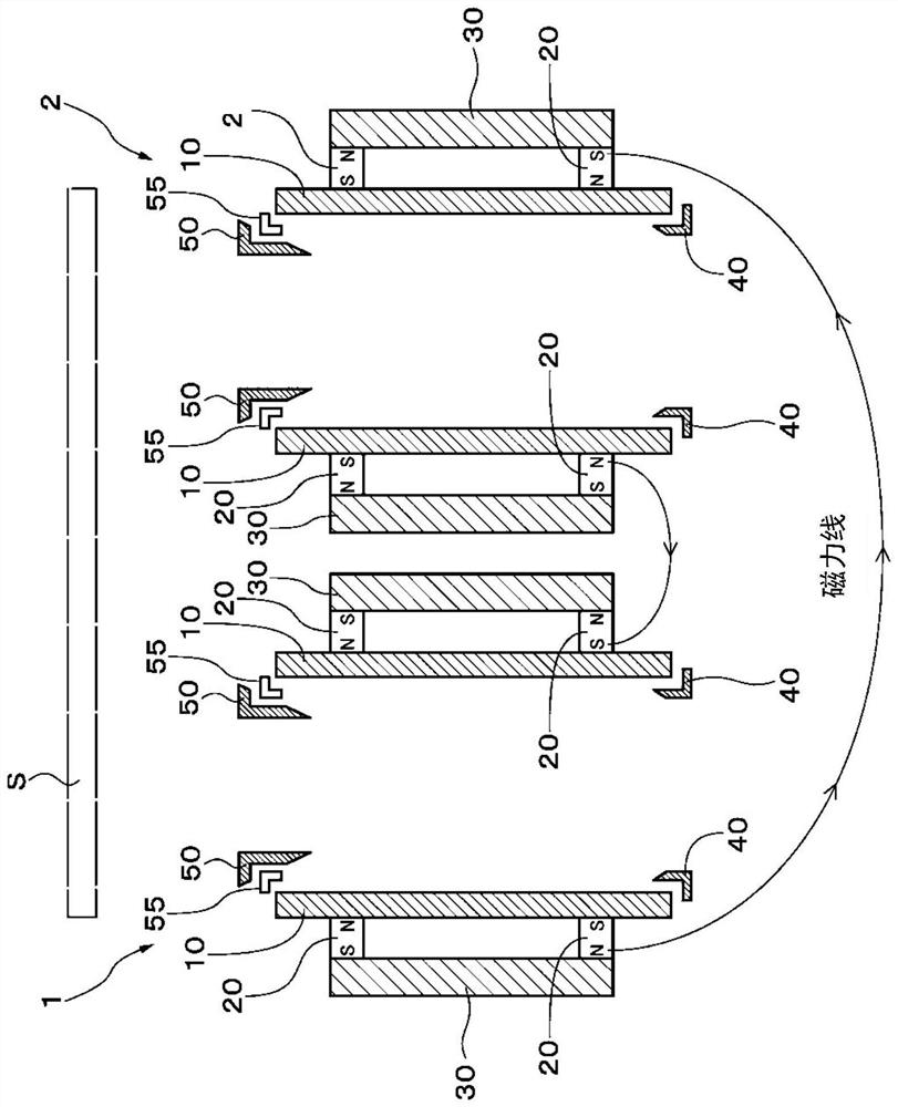
[0074] figure 1 and figure 2 It is a longitudinal sectional view and a plan view showing the sputtering apparatus according to the first embodiment, showing the structure near the sputtering cathode assembly provided inside the vacuum container of the sputtering apparatus. figure 1 is along figure 2 The cross-sectional view of the XX line.

[0075] Such as figure 1 and figure 2 As shown, in this sputtering device, a plurality of sputtering cathodes are arranged side by side on a horizontal plane, and these sputtering cathodes form a sputtering cathode assembly. The number of sputtering cathodes constituting the sputtering cathode assembly is appropriately selected according to the size of the substrate to be film-formed, the film-forming method, and the like. exist figure 1 and figure 2 In , as an example, only a pair of sputtering cathodes 1 and 2 adjacent to each other are shown, but it is not limited thereto. The distance between th...

no. 2 approach

[0092] [sputtering device]

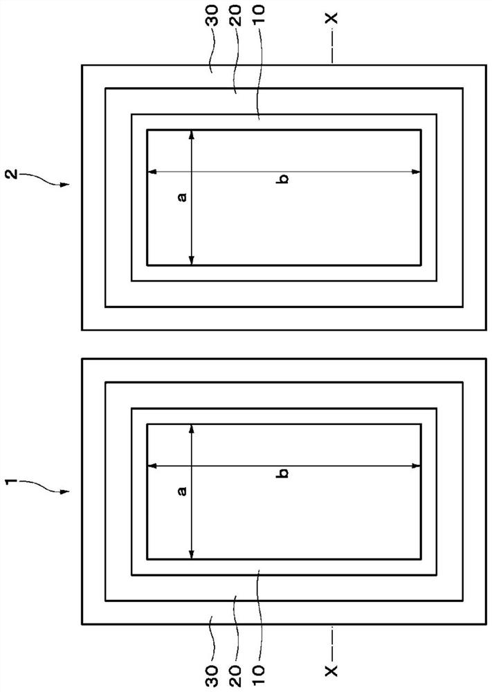
[0093] The sputtering apparatus according to the second embodiment differs from the sputtering apparatus according to the first embodiment in that as the sputtering target 10 Figure 11 The sputtering target shown. That is, if Figure 11 As shown, the sputtering target 10 is composed of a pair of long side portions facing each other in parallel and a semicircular portion connected to these long side portions. Both the permanent magnet 20 provided outside the sputtering target 10 and the yoke 30 provided outside the permanent magnet 20 have the same shape as the sputtering target 10 . Other configurations of the sputtering device are the same as those of the sputtering device according to the first embodiment.

[0094] [Film formation method using a sputtering device]

[0095] The method of forming a film using this sputtering device is the same as that of the first embodiment.

[0096] According to this second embodiment, the same advantages a...

no. 3 approach

[0098] [sputtering device]

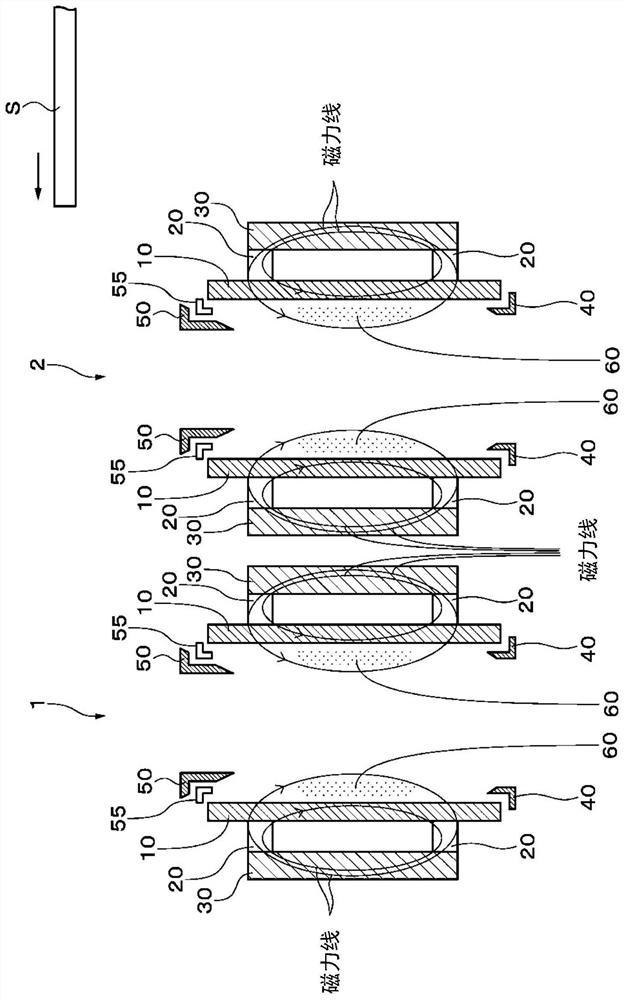
[0099] Figure 12 and Figure 13 It is a longitudinal sectional view and a plan view showing a sputtering apparatus according to a third embodiment, and shows a structure near a sputtering cathode assembly provided inside a vacuum container of the sputtering apparatus. Figure 13 is along Figure 12 A cross-sectional view of the Y-Y line.

[0100] Such as Figure 12 and Figure 13 As shown, in the sputtering device, a plurality of sputtering cathodes are arranged side by side on a vertical plane, and these sputtering cathodes form a sputtering cathode assembly. The number of sputtering cathodes constituting the sputtering cathode assembly is appropriately selected according to the desired film formation speed and the like. exist Figure 12 and Figure 13 In , as an example, only a pair of sputtering cathodes 1 and 2 adjacent to each other are shown, but it is not limited thereto. The distance between the sputtering cathodes 1 and 2 is appr...


PUM


Abstract

The present invention addresses the problem of providing a sputtering cathode and a sputtering device using this sputtering cathode by which a film can be deposited on various kinds of workpieces, including flat workpieces, not only at a sufficiently high deposition rate with low impact but also with high sputtering target utilization efficiency. The sputtering cathode comprises a sputtering target 10 which has a tubular shape with a cross section having an opposing pair of long sides and which is set so that the erosion surface of the sputtering target 10 is inward-facing; additionally a magnetic circuit is disposed along the sputtering target 10, and the pair of long sides are constituted by cylindrical rotary targets 11, 12. The rotary targets have magnetic circuits therein and are configured such that cooling water flows therethrough. The magnetic circuits are disposed parallel to the central axis of the rotary targets and have a rectangular cross-section with long sides perpendicular to the radial direction of the rotary targets.

Description

technical field [0001] The present invention relates to a sputtering cathode, a sputtering cathode assembly, and a sputtering device, and is applicable to the manufacture of various devices in which a thin film is formed by a sputtering method. Background technique [0002] Conventionally, in the process of forming electrodes in various devices such as semiconductor devices, solar cells, liquid crystal displays, and organic EL displays, vacuum vapor deposition devices have been widely used for film formation of electrode materials. However, since it is difficult to control the film thickness distribution spatially and temporally by the vacuum evaporation method, it is required to form the electrode material into a film by the sputtering method. [0003] Conventionally, as a sputtering apparatus, a parallel-plate magnetron type sputtering apparatus, an RF type sputtering apparatus, an opposing target type sputtering apparatus, etc. are known. Among them, in the opposing targ...

Claims


Application Information

Patent Timeline
IPC IPC(8): C23C14/34C23C14/35H05H1/46
CPCC23C14/3407C23C14/352H01J37/3405H01J37/3417H01J37/3423H05H1/466H05H1/50H05H2245/40H01J37/3447H01J37/3467H01J37/345C23C14/35
Inventor 岩田宽
Owner KEIHIN RAM TECH
Why Eureka
Try Eureka