Semiconductor material processing system

A material processing and semiconductor technology, applied in the direction of polycrystalline material growth, crystal growth, stone processing equipment, etc., can solve the problems of increasing the difficulty of cleaning the outer surface of graphite crucible, increasing the risk factor of crystal manufacturing, and inconvenient cleaning and collection of silica gel film. Achieve the effect of reducing the difficulty of cleaning and measuring, solving the inconvenience of measuring and cleaning, and moving up and down stably

Active Publication Date: 2020-12-04
深圳市凯新达电子有限公司
View PDF4 Cites 0 Cited by
  • Summary
  • Abstract
  • Description
  • Claims
  • Application Information

AI Technical Summary

Problems solved by technology

[0004] The present invention provides a semiconductor material processing system, which can effectively solve the problem that the graphite crucible inside the crystal furnace is easily deformed due to high temperature during the actual use of the existing crystal furnace, and the graphite crucible The slight deformation of the outer w

Method used


Image

  • Semiconductor material processing system
  • Semiconductor material processing system
  • Semiconductor material processing system

Examples


Embodiment

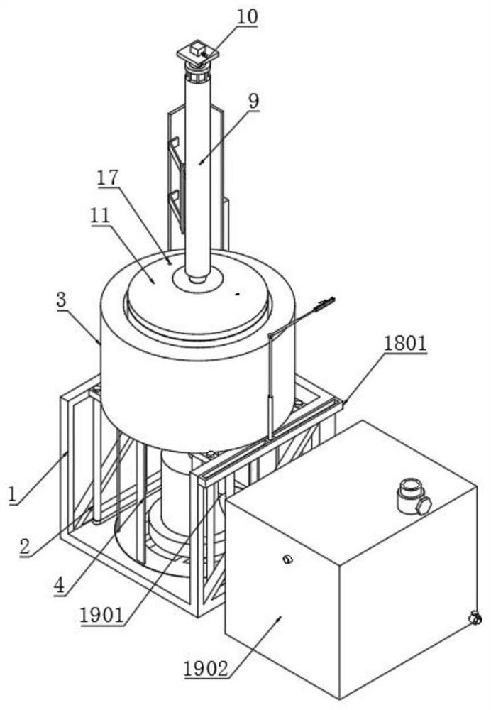
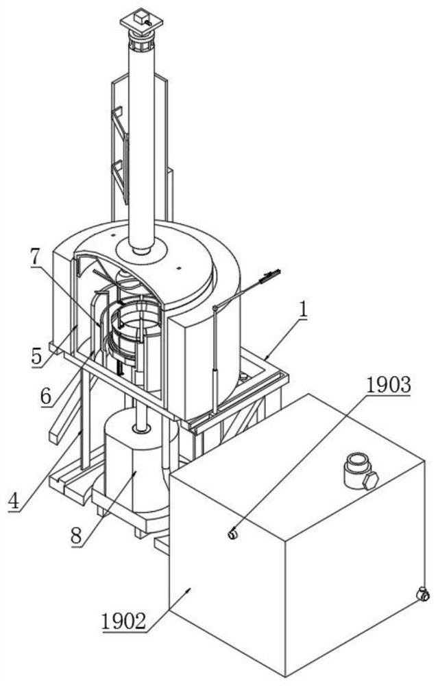
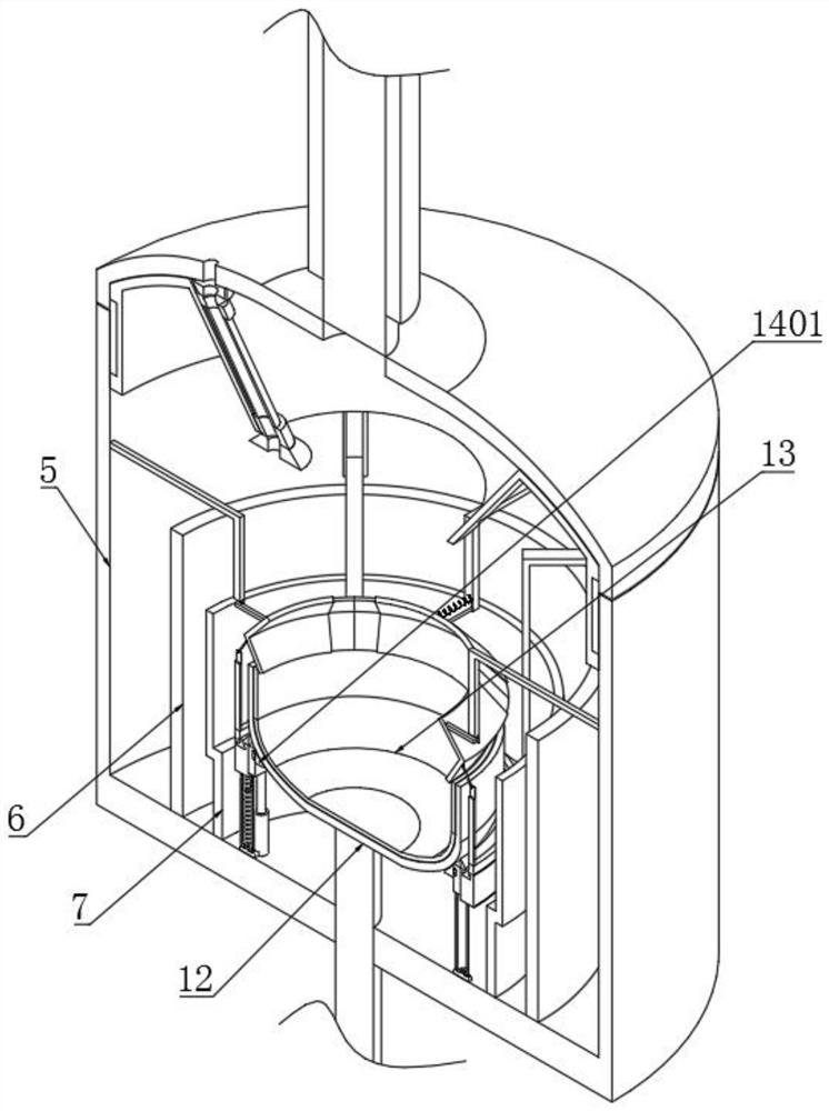
[0043] Example: such as Figure 1-15 As shown, the present invention provides a technical solution, a semiconductor material processing system, including a support 1, support rods 2 are fixedly installed at the four corners of the bottom end of the support 1, and support rods 2 are fixedly installed on the top of the support rod 2 and the top edge of the support 1 The protective cover 3, the fixed rod 4 is equidistantly installed in the middle part of the bottom end of the support 1, the cold water jacket 5 is fixedly installed in the middle part of the top end of the fixed rod 4, and the heat insulation plate 6 is fixedly installed at the bottom end of the inner wall of the cold water jacket 5, and the inner wall of the cold water jacket 5 corresponds to heat insulation A graphite resistance heater 7 is fixedly installed on one side of the plate 6, a bottom rotating elevator 8 is fixedly installed in the middle part of the bottom end of the cold water jacket 5, a graphite cruc...


PUM


Abstract

The invention discloses a semiconductor material processing system which comprises a support, supporting rods are fixedly installed at the four corners of the bottom end of the support correspondingly, protective sleeves are fixedly installed at the top ends of the supporting rods and the edges of the top end of the support correspondingly, and fixing rods are installed in the middle of the bottomend of the support at equal intervals, so that the moving stability of a graphite crucible can be improved by a rotation positioning cleaning mechanism, meanwhile, the outer surface of the graphite crucible can be measured and cleaned, so that the cleaning and measuring difficulty of the outer surface of the graphite crucible is reduced, and the phenomenon that in the prior art, the graphite crucible is prone to shaking during running is avoided,meanwhile, the problem that the graphite crucible is inconvenient to measure and clean in the prior art is solved, so that the operation efficiency of personnel is improved, the safety of the graphite crucible during operation can be improved on the premise that the normal use of the graphite crucible is not influenced, the safety coefficient of the device is increased, the damage rate of the device is reduced, and the production cost is reduced. Therefore, the service life of the device is prolonged.

Description

technical field [0001] The invention relates to the technical field of semiconductor material production, in particular to a semiconductor material processing system. Background technique [0002] Semiconductors refer to materials whose conductivity is between conductors and insulators at room temperature. Semiconductors are used in integrated circuits, consumer electronics, communication systems, photovoltaic power generation, lighting, high-power power conversion and other fields. For example, diodes are devices made of semiconductors. , no matter from the perspective of technology or economic development, the importance of semiconductors is very huge. The core units of most electronic products, such as computers, mobile phones or digital recorders, are closely related to semiconductors. , common semiconductor materials include silicon, germanium, gallium arsenide, etc., silicon is the most influential one in the application of various semiconductor materials, and silicon ...

Claims


Application Information

Patent Timeline
IPC IPC(8): C30B29/06C30B15/00C30B15/12C30B15/20B28D5/04B28D5/00
CPCC30B29/06C30B15/00C30B15/12C30B15/20B28D5/04B28D5/0058
Inventor 杨文伟
Owner 深圳市凯新达电子有限公司
Why Eureka
Try Eureka