Supercharge Your Innovation With Domain-Expert AI Agents!

Film bulk acoustic resonator and manufacturing method thereof

A thin-film bulk acoustic wave and manufacturing method technology, applied in electrical components, impedance networks, etc., can solve problems such as the inability to further improve the quality factor and the inability to meet high-performance radio frequency systems, so as to improve acoustic wave loss, improve device performance, and block shear waves. effect of loss

Pending Publication Date: 2020-12-04
NINGBO SEMICON INT CORP
View PDF0 Cites 3 Cited by
  • Summary
  • Abstract
  • Description
  • Claims
  • Application Information

AI Technical Summary

Problems solved by technology

[0004] However, the quality factor (Q) of the cavity-type thin-film bulk acoustic resonator produced at present cannot be further improved, so it cannot meet the needs of high-performance radio frequency systems

Method used


Image

  • Film bulk acoustic resonator and manufacturing method thereof
  • Film bulk acoustic resonator and manufacturing method thereof
  • Film bulk acoustic resonator and manufacturing method thereof

Examples


Embodiment 1

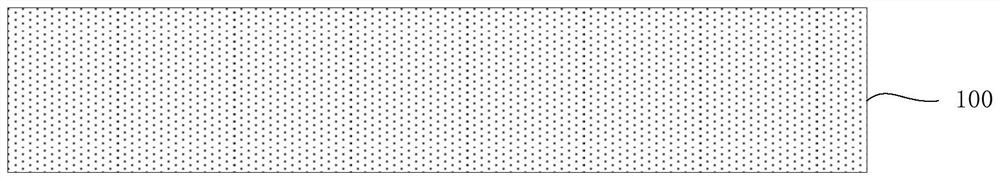
[0050] refer to image 3 and Figure 4 , performing steps S01 and S02 , providing a first substrate 100 , and forming a piezoelectric stack structure 120 on the first substrate 100 . The piezoelectric stack structure 120 includes a second electrode layer 102, a piezoelectric layer 103 and a first electrode layer 104, wherein the piezoelectric layer 103 is located between the first electrode layer 104 and the second electrode layer 102, and the first electrode layer 104 is opposite to the second electrode layer 102 .

[0051] The material of the first substrate can be at least one of the materials mentioned below: silicon (Si), germanium (Ge), silicon germanium (SiGe), silicon carbon (SiC), silicon germanium carbon (SiGeC), arsenic Indium (InAs), gallium arsenide (GaAs), indium phosphide (InP) or other III / V compound semiconductors, including multilayer structures composed of these semiconductors, or silicon-on-dielectric (SOI), dielectric Silicon-on-layer (SSOI), silicon-ge...

Embodiment 2

[0066] refer to Figure 3-Figure 6 and Figure 13-Figure 19 , steps S01, S02, and S03 are the same as in Embodiment 1, and step S03 also includes, after the first electrode layer 104 is patterned, forming a first The number and depth of the grooves 106 and the first grooves 106 are not limited, and can be set according to different technical requirements. In this example, the number of the first groove 106 is one, the depth is the thickness of the piezoelectric layer 103, and the first groove 106 surrounds a part of the outer circumference of the first electrode 104'. The first groove 106 is ring-shaped with an opening, and the first electrode 104' is connected to the supporting layer 105 through the opening, so as to lead the first electrode 104' out and form a first pad in the non-effective resonance area. The method for forming the first groove 106 is similar to the method for forming the cavity 110a, and dry etching or a combination of wet etching and dry etching can be ...

Embodiment 3

[0069] see Figure 20 , on the basis of Example 2, after step S08 is performed, further comprising, forming a second groove 107 in the exposed piezoelectric layer 103 near the edge of the second electrode 102' in the area where the second electrode 102' is removed The structure and formation process of the second groove 107 refer to the relevant content of the first groove in Embodiment 2. In this example, there is one second groove, the depth is the thickness of the piezoelectric layer, and the second groove 107 surrounds the periphery of a portion of the second electrode 102'. The second groove 107 is ring-shaped with an opening, and the second electrode 102' is connected to the support layer 105 through the opening, so as to lead the second electrode 102' out and form a second pad 112 in the non-effective resonance area. In this example, the cross-sectional shape of the second groove 107 is a trapezoid with a narrow bottom and a wide top, and the angle between the side wal...


PUM


Abstract

The invention discloses a film bulk acoustic wave resonator and a manufacturing method thereof. The manufacturing method of the film bulk acoustic wave resonator comprises the following steps: providing a first substrate; forming a piezoelectric laminated structure on the first substrate, wherein the piezoelectric laminated structure comprises a second electrode layer, a piezoelectric layer and afirst electrode layer which are laminated in sequence; patterning the first electrode layer to form a first electrode, and enabling a part of the edge of the first electrode in the effective resonanceregion to be cut off above the cavity; after the first electrode is formed, forming a supporting layer on the piezoelectric laminated structure; forming a cavity penetrating through the supporting layer in the supporting layer; bonding a second substrate on the supporting layer, wherein the second substrate covers the cavity; after bonding the second substrate, removing the first substrate; and patterning the second electrode layer to form a second electrode, so that part of the edge of the second electrode in an effective resonance region is cut off above the cavity, and the first electrodeand the second electrode outside the effective resonance region have no overlapped region in the direction perpendicular to the piezoelectric layer.

Description

technical field [0001] The invention relates to the field of semiconductor device manufacturing, in particular to a thin-film bulk acoustic wave resonator and a manufacturing method thereof. Background technique [0002] Since the development of analog RF communication technology in the early 1990s, RF front-end modules have gradually become the core components of communication equipment. Among all RF front-end modules, filters have become the components with the strongest growth momentum and the greatest development prospects. With the rapid development of wireless communication technology and the maturity of 5G communication protocols, the market has also put forward stricter standards for the performance of RF filters in all aspects. The performance of a filter is determined by the resonator units that make up the filter. Among the existing filters, the film bulk acoustic resonator (FBAR) has the characteristics of small size, low insertion loss, large out-of-band suppr...

Claims


Application Information

Patent Timeline
IPC IPC(8): H03H3/02H03H9/02H03H9/05H03H9/13
CPCH03H3/02H03H9/02015H03H9/02047H03H9/0504H03H9/131H03H9/132H03H2003/023
Inventor 杨国煌
Owner NINGBO SEMICON INT CORP
Features
  • R&D
  • Intellectual Property
  • Life Sciences
  • Materials
  • Tech Scout
  • Unparalleled Data Quality
  • Higher Quality Content
  • 60% Fewer Hallucinations
Learn More