TFT array substrate structure and manufacturing method

A fabrication method and array substrate technology, which are applied in semiconductor/solid-state device manufacturing, electrical components, electrical solid-state devices, etc., can solve the problems affecting the driving current of IGZOTFT, the increase of Schottky contact resistance, and the reduction of carrier mobility, etc. problem, to achieve the effect of saving cost output, reducing electrical drift of the device, and fine grain

Pending Publication Date: 2020-12-18
FUJIAN HUAJIACAI CO LTD
View PDF0 Cites 3 Cited by
  • Summary
  • Abstract
  • Description
  • Claims
  • Application Information

AI Technical Summary

Problems solved by technology

[0004] IGZO films are usually prepared by magnetron sputtering in the prior art, but the IGZO films usually contain a large number of oxygen vacancies. On the one hand, the oxygen vacancies increase the carrier concentration of the IGZO film, but reduce the carrier density. Mobility; At the same time, the process of IGZO film coating, exposure, development and stripping, during the process of photoresist stripping, the IGZO film will be soaked in oxalic acid in the stripping solution, and the oxalic acid will destroy the IGZO film. There are a large number of interface lattice defects. Increase the oxygen vacancies in IGZO, reduce the mobility of carriers, and increase the Schottky contact resistance formed by the contact between IGZO and the metal source and drain due to interface lattice defects, which in turn affects the driving current of IGZO TFT. overall degraded device performance

Method used


Image

  • TFT array substrate structure and manufacturing method
  • TFT array substrate structure and manufacturing method
  • TFT array substrate structure and manufacturing method

Examples


Embodiment Construction

[0036] In order to explain in detail the technical content, structural features, achieved goals and effects of the technical solution, the following will be described in detail in conjunction with specific embodiments and accompanying drawings.

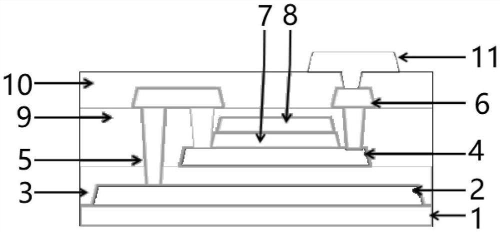
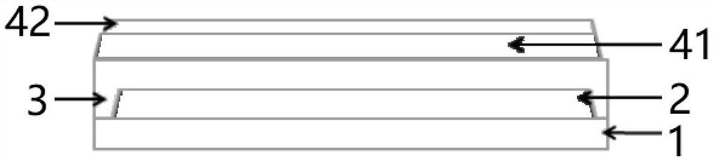
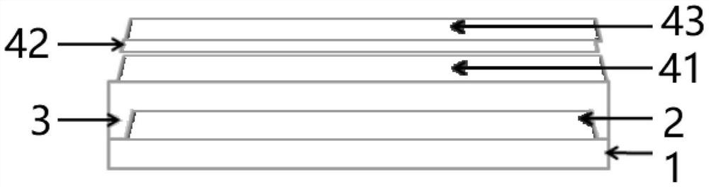
[0037] see Figure 1 to Figure 5, the present embodiment provides a method for manufacturing a TFT array substrate, comprising the steps of: depositing a light-shielding layer 2 on the substrate 1, and fabricating a buffer layer 3 on the light-shielding layer 2; fabricating a first buffer layer 3 on the buffer layer 3 active layer 41, and make a second active layer 42 on the first active layer 41; pattern the first active layer 41 and the second active layer 42 to form an active layer film 4; The active layer film 4 includes: a first active layer 41 and a second active layer 42; a gate insulating layer 7 is formed on the first active layer 41, and a gate insulating layer 7 is formed on the gate insulating layer 7 metal gate layer 8; ...


PUM


Abstract

The invention discloses a TFT array substrate structure and a manufacturing method. The method comprises the steps: depositing a shading layer on a substrate, and manufacturing a buffering layer; manufacturing a first active layer and a second active layer; patterning the first active layer and the second active layer; manufacturing a gate insulating layer on the first active layer, and manufacturing a metal gate layer on the gate insulating layer; manufacturing a passivation layer, a first through hole, a second through hole and a third through hole, wherein the second through hole and the third through hole are formed in the two sides of the metal gate layer respectively; manufacturing a metal source electrode and a metal drain electrode, wherein the metal source electrode is connected with the shading layer through the first through hole, the metal source electrode is connected with the first active layer through the second through hole, and the metal drain electrode is connected with the first active layer through the third through hole; manufacturing a flat layer, and manufacturing a fourth through hole; and manufacturing an electrode layer, and connecting the electrode layerwith the metal drain. By means of the process, damage to the first active layer in the preparation process of the TFT array substrate is reduced, so that the effect of protecting the first active layer thin film is achieved, meanwhile, electrical drifting of a device is reduced, and the performance of the thin film transistor is improved.

Description

technical field [0001] The invention relates to the technical field of TFT array substrates, in particular to a TFT array substrate structure and a manufacturing method. Background technique [0002] Top-gate thin-film transistors have lower parasitic capacitance and better ductility because there is no overlap between the source-drain electrodes and the gate, and can avoid A-Si TFT due to gate and source-drain electrodes. The overlapping area is large, resulting in a large parasitic capacitance, so the delay in the signal transmission process can be reduced in the top gate (Top-gate) thin film transistor, and the self-aligned preparation method is used to facilitate the preparation of short-channel devices. And the metal oxide IGZO is used as the active layer, which has high electron mobility and is conducive to improving device characteristics. The top-gate thin film transistor structure will become the development trend of the display field in the future; [0003] IGZO (...

Claims


Application Information

Patent Timeline
Patent Type & Authority Applications(China)
IPC IPC(8): H01L21/77H01L27/12
CPCH01L27/1225H01L27/127
Inventor 温质康苏智昱乔小平
Owner FUJIAN HUAJIACAI CO LTD
Why Eureka
Try Eureka