Polishing device for semiconductor preparation

A polishing device and semiconductor technology, used in grinding/polishing safety devices, grinding drive devices, grinding/polishing equipment, etc., can solve the physical health injury of workers, low polishing efficiency of polishing devices, difficult to polish semiconductor products, etc. problem, to reduce the probability of shaking, improve polishing accuracy, and facilitate the effect of fixing work

Active Publication Date: 2020-12-25
JIANGSU ETERN +2
View PDF6 Cites 4 Cited by
  • Summary
  • Abstract
  • Description
  • Claims
  • Application Information

AI Technical Summary

Problems solved by technology

[0004] Aiming at the deficiencies of the prior art, the present invention provides a polishing device for semiconductor preparation, which solves the problem that the polishing device for semiconductor preparation in the prior art has low polishing efficiency, it is difficult to polish long semiconductor products, and the dust generated during the polishing process It is easy to cause pollution to the working environment and cause certain harm to the health of the staff

Method used


Image

  • Polishing device for semiconductor preparation
  • Polishing device for semiconductor preparation
  • Polishing device for semiconductor preparation

Examples


Embodiment Construction

[0056] The following will clearly and completely describe the technical solutions in the embodiments of the present invention with reference to the accompanying drawings in the embodiments of the present invention. Obviously, the described embodiments are only some, not all, embodiments of the present invention. Based on the embodiments of the present invention, all other embodiments obtained by persons of ordinary skill in the art without making creative efforts belong to the protection scope of the present invention.

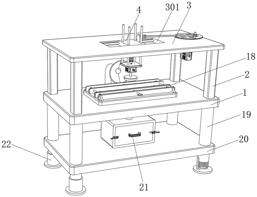
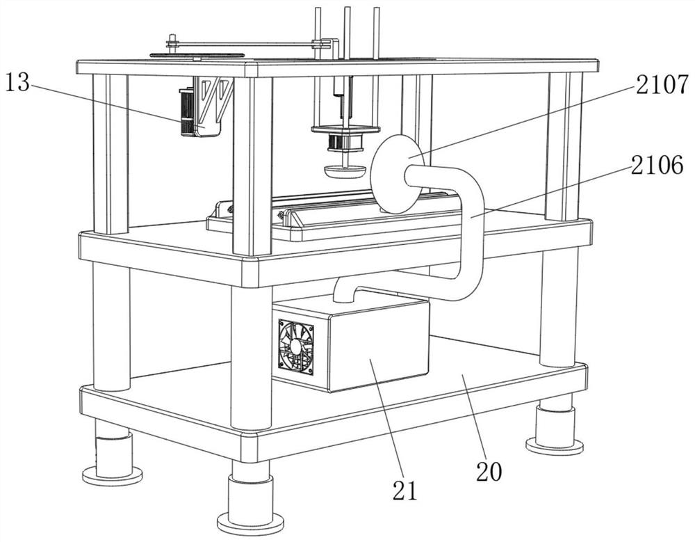
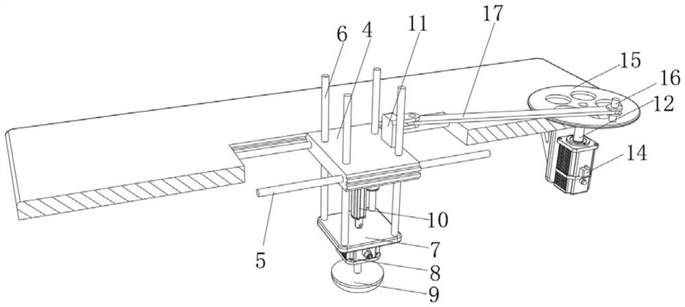
[0057] see Figure 1-5 , the present invention provides a technical solution: a polishing device for semiconductor preparation, including a workbench 1, the four corners of the upper surface of the workbench 1 are fixedly connected with a first column 2, and the upper surface of the first column 2 is fixedly connected with a top plate 3, Top plate 3 upper surface middle part is provided with slide groove 301, and slide groove 301 inner wall is slidingly connec...


PUM


Abstract

The invention relates to the technical field of semiconductor processing equipment, and discloses a polishing device for semiconductor preparation. The polishing device comprises a workbench; first stand columns are fixedly connected to the four corners of the upper surface of the workbench; a top plate is fixedly connected to the upper surfaces of the first stand columns; a sliding groove is formed in the middle of the upper surface of the top plate; a sliding platform is glidingly connected to the inner wall of the sliding groove; and sliding rods are inserted in the front side and the backside of the right side surface of the sliding platform. According to the polishing device for semiconductor preparation, a second driving motor, a rotating shaft, a rotating disc, a crank, a connecting plate and the sliding platform are used in cooperation, the second driving motor drives the rotating disc to rotate through the rotating shaft, and the rotating disc drives the sliding table to moveleftwards and rightwards through the crank, so that the polishing area of the device for semiconductor products is further increased, the device can be used for polishing relatively-long semiconductor products, and the working efficiency of the device is further improved.

Description

technical field [0001] The invention relates to the technical field of semiconductor processing equipment, in particular to a polishing device for semiconductor preparation. Background technique [0002] Semiconductor materials are a class of electronic materials that have semiconductor properties and can be used to make semiconductor devices and integrated circuits. Due to their stable structure, excellent electrical properties, and low cost, semiconductor materials are used to manufacture fields widely used in modern electronic equipment. Effect transistors, in semiconductor manufacturing, abrasive processing such as grinding and grinding is a necessary way to produce semiconductor wafers. However, grinding and grinding will cause the surface integrity of single crystal silicon wafers to deteriorate. Therefore, polishing and planarization are very important for the production of microelectronic components. It is very important; general semiconductor polishing equipment pol...

Claims


Application Information

Patent Timeline
Patent Type & Authority Applications(China)
IPC IPC(8): B24B29/02B24B55/06B24B27/02B24B27/00B24B49/00B24B47/22B24B47/12B24B41/00B24B41/06B01D46/10
CPCB24B29/02B24B55/06B24B27/02B24B27/0046B24B49/006B24B47/22B24B47/12B24B41/007B24B49/00B24B41/06B01D46/10
Inventor 陈玉琼
Owner JIANGSU ETERN
Why Eureka
Try Eureka