
Ultrahigh-precision multilayer film thickness drift error calibration method

A technology of drift error and calibration method, applied in the direction of testing optical properties, etc., can solve problems such as the boundary of difficult film thickness calculation, the inability to measure thickness error, and the accuracy cannot reach resolution, etc., to achieve small influence of instrument conditions and high characterization accuracy , highly controllable effect

Active Publication Date: 2021-01-05
TONGJI UNIV
View PDF6 Cites 2 Cited by
  • Summary
  • Abstract
  • Description
  • Claims
  • Application Information

AI Technical Summary

Problems solved by technology

But even if the transmission electron microscope is used, although its ideal spatial resolution can reach 0.1nm, when the actual film grows, there will be atomic diffusion and mixing on the interface and surface, so it is difficult to accurately determine the boundary of film thickness calculation, and the calibration accuracy is far from reaching its resolution, and it is impossible to measure the thickness error of tens of picometers

Method used

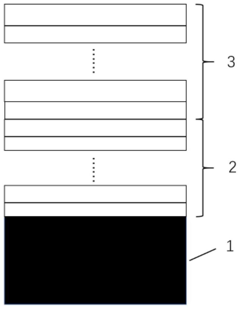
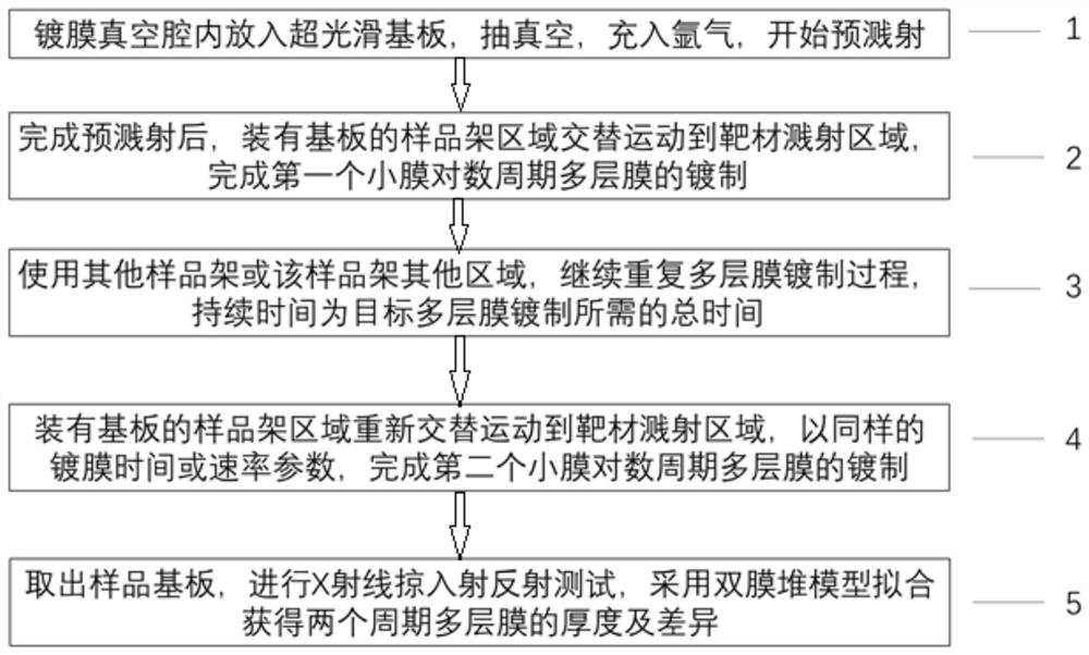
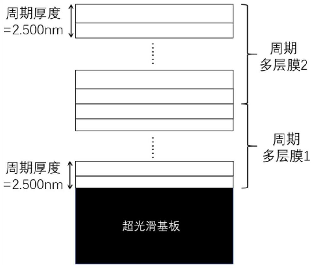

Image

  • Ultrahigh-precision multilayer film thickness drift error calibration method
  • Ultrahigh-precision multilayer film thickness drift error calibration method
  • Ultrahigh-precision multilayer film thickness drift error calibration method

Examples


Embodiment 1

[0037] In this embodiment, the target period multilayer film is palladium / boron carbide, the period thickness is 2.5nm, the total number of film pairs of the finished multilayer film is 150 pairs, and the length of the multilayer film reflector for the synchrotron radiation light source monochromator is generally 300mm. It takes 25-30 hours to complete the plating of this large-scale palladium / boron carbide multilayer film mirror by using magnetron sputtering technology. During the long-term sputtering process, due to the change of the voltage and current of the palladium and boron carbide target guns, and the change of the depth of the etching ring on the target surface, the film deposition rate will drift slightly, and the general drift range is 1% to 5%. about. According to calculations, in order to obtain high reflectivity of the multi-layer film, the thickness drift range of all film layers in the structure cannot exceed 2%, corresponding to an absolute thickness drift va...


PUM

PropertyMeasurementUnit
thicknessaaaaaaaaaa
thicknessaaaaaaaaaa
surface roughnessaaaaaaaaaa

Abstract

The invention relates to an ultrahigh-precision multilayer film thickness drift error calibration method, which comprises the steps of of alternately moving a substrate to a sputtering region of two target materials for plating a multilayer film, and plating a first periodic multilayer film; enabling the substrate to be far away from the sputtering region, continuing sputtering the target materials, and simulating the plating process of the target periodic multilayer film; alternately moving the substrate plated with the first periodic multilayer film to the sputtering region again, and plating a second periodic multilayer film to form a calibration sample; and performing an X-ray grazing incidence reflection test on the plated calibration sample under fixed X-ray energy to obtain a test reflectivity curve, and obtaining a multilayer film drift error from the beginning to the end based on comparison between the test reflectivity curve and the simulated reflectivity curve, wherein the number of film pairs of the first periodic multilayer film and the second periodic multilayer film is 1 / 10-1 / 5 of the number of film pairs of the target periodic multilayer film. Compared with the prior art, the method has the advantages of high precision, small influence of instrument conditions and the like.

Description

technical field [0001] The invention belongs to the technical field of optical thin films, and in particular relates to an ultra-high-precision multilayer film thickness drift error calibration method, in particular to the calibration of high-precision film thickness errors of large-film logarithmic X-ray multilayer films. Background technique [0002] The one-dimensional nanometer (nm) multilayer film structure is an important reflection element in the X-ray band, which can realize the reflection and monochromatization of X-rays outside the total external reflection region. A conventional multilayer film is composed of an absorbing layer with a high atomic number and a spacer layer with a low atomic number, and the reflection bandwidth (ΔE / E) is about 2% to 5%. With the development of applications such as synchrotron radiation light source devices, the requirements for the monochromatization performance of multilayer films are getting higher and higher, and high-resolution ...

Claims


Application Information

Patent Timeline
Patent Type & Authority Applications(China)
IPC IPC(8): G01M11/02
CPCG01M11/02
Inventor 王占山黄秋实齐润泽张众
Owner TONGJI UNIV
Learn More