

A method for improving in-plane uniformity of a critical dimension of a device
A key size, uniform technology, applied in the photoengraving process of pattern surface, semiconductor/solid-state device testing/measurement, instrument, etc., can solve the problem of long correction period and so on
- Summary
- Abstract
- Description
- Claims
- Application Information
AI Technical Summary
Problems solved by technology
Method used
Image

Examples
Embodiment Construction
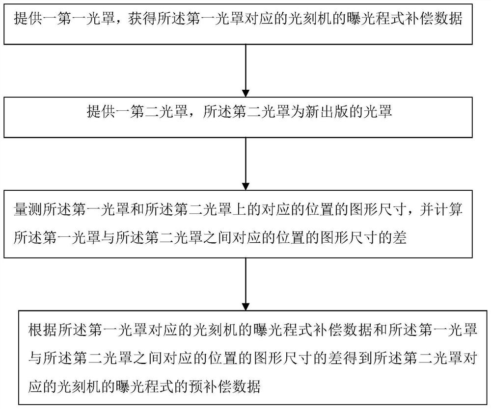
[0013] The technical solutions in the present invention will be clearly and completely described below in conjunction with the accompanying drawings. Apparently, the described embodiments are part of the embodiments of the present invention, not all of them. Based on the embodiments of the present invention, all other embodiments obtained by persons of ordinary skill in the art without making creative efforts belong to the protection scope of the present invention.
[0014] It should be understood that the invention can be embodied in different forms and should not be construed as limited to the embodiments set forth herein. Rather, these embodiments are provided so that this disclosure will be thorough and complete, and will fully convey the scope of the invention to those skilled in the art. It should be understood that although the terms first, second, third etc. may be used to describe various elements, components, regions, layers, steps and / or sections, these elements, co...
PUM
 Abstract
Description
Claims
Application Information