

On-chip mode division multiplexing device based on reflection effect
A technology of mode division multiplexing and reflection effect, applied in instruments, optical components, optical waveguides and light guides, etc., can solve the problems of large device size, wavelength sensitivity, and small tolerance of manufacturing errors, and achieve large working bandwidth, simple preparation, Produces effects with high tolerance to errors
- Summary
- Abstract
- Description
- Claims
- Application Information
AI Technical Summary
Problems solved by technology
Method used
Image

Examples
Embodiment Construction
[0025] The preferred embodiments of the present invention will be further described in detail below.
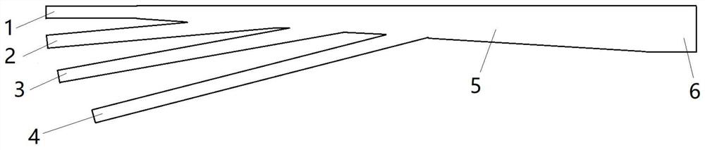
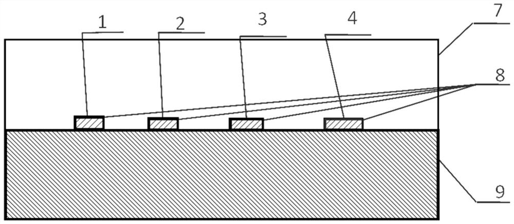
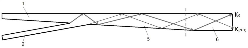
[0026] Such as figure 1 and figure 2 As shown, an on-chip mode division multiplexing device based on the reflection effect, this embodiment has four modes on the chip, including TE0 mode, TE1 mode, TE2 mode and TE3 mode. The device includes a base layer 9, an optical waveguide layer 8 and a cladding layer 7, the optical waveguide layer 8 includes 4 single-mode waveguides, a tapered waveguide 5 and a wide multi-mode waveguide 6. The tail ends of the 4 single-mode waveguides It is connected to different positions on the same side of the tapered waveguide 5 , and the tail end of the tapered waveguide 5 is connected to the wide multimode waveguide 6 .
[0027] Wherein, the four single-mode waveguides include the first single-mode waveguide 1 (TE0 mode channel), the second single-mode waveguide 2 (TE1 mode channel), the third single-mode waveguide 3 (TE2 mode channel), the four...
PUM
 Abstract
Description
Claims
Application Information