Method for reducing stress of passivation layer and passivation layer stress buffer structure

A technology of stress buffering and passivation layer, which can be used in the manufacture of electrical components, electrical solid-state devices, semiconductor/solid-state devices, etc., and can solve problems such as pinholes or cracks

Pending Publication Date: 2021-01-15
SHANGHAI HUAHONG GRACE SEMICON MFG CORP
View PDF0 Cites 3 Cited by
  • Summary
  • Abstract
  • Description
  • Claims
  • Application Information

AI Technical Summary

Problems solved by technology

Therefore, there is a need for a method for reducing the stress of the passivation layer to solve the problem of defects such as pinholes or cracks

Method used


Image

  • Method for reducing stress of passivation layer and passivation layer stress buffer structure
  • Method for reducing stress of passivation layer and passivation layer stress buffer structure
  • Method for reducing stress of passivation layer and passivation layer stress buffer structure

Examples


Embodiment Construction

[0035] The specific implementation manner of the present invention will be described in more detail below with reference to schematic diagrams. The advantages and features of the present invention will be more apparent from the following description. It should be noted that all the drawings are in a very simplified form and use imprecise scales, and are only used to facilitate and clearly assist the purpose of illustrating the embodiments of the present invention.

[0036] Figure 4 A flow chart of the method for reducing the stress of the passivation layer provided in this embodiment. refer to Figure 4 , this embodiment provides a method for reducing the stress of the passivation layer, including:

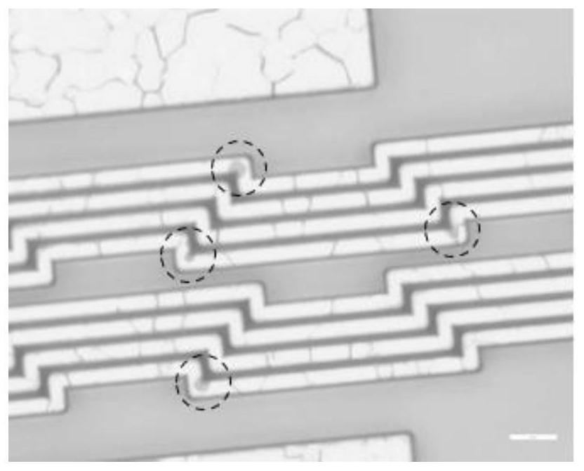
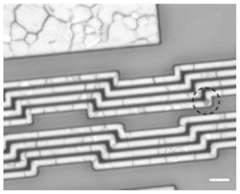
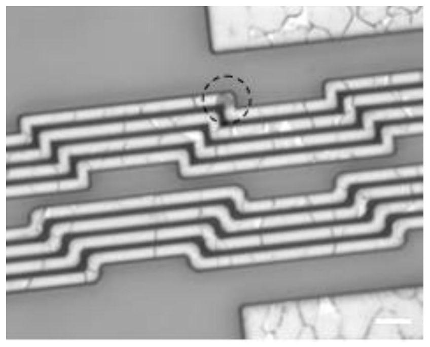
[0037] Step S01: Provide a design layout for defining the structure of a belt-shaped metal layer, the belt-shaped metal layer includes at least one corner area, and the corner area includes a first corner greater than 180° and a first corner less than 180° a second corner, an...


PUM


Abstract

The invention provides a method for reducing the stress of a passivation layer and a passivation layer stress buffer structure. The method for reducing the stress of the passivation layer comprises the steps of providing a design layout for defining the structure of a strip-shaped metal layer, the strip-shaped metal layer comprising at least one corner area, the corner area comprising a first corner larger than 180 degrees and a second corner smaller than 180 degrees, and the sum of the first corner and the second corner being 360 degrees; modifying the first corner and the second corner in the design layout to form stress buffer structures at the first corner and the second corner; and sequentially forming a metal layer and a passivation layer on the surface of a substrate according to the design layout, wherein passivation layer stress buffer structures are formed at the first corner and the second corner of the passivation layer. According to the method for reducing the stress of the passivation layer, the structure of the passivation layer is changed by changing the structure of the strip-shaped metal layer, so that the internal stress influence of the passivation layer is relieved, and defects at special positions of the passivation layer are reduced or avoided.

Description

technical field [0001] The invention relates to the technical field of semiconductors, in particular to a method for reducing the stress of a passivation layer and a stress buffer structure of the passivation layer. Background technique [0002] For integrated circuits with high performance and high reliability, the passivation of the chip surface has become one of the essential process measures. The passivation layer is mainly used for electrical isolation between devices and wiring, and to isolate the device from the surrounding environment atmosphere, so as to enhance the device's ability to block external ion contamination, protect the internal interconnection of the device, and prevent mechanical damage and chemical damage. [0003] The type and structure of the passivation layer have a great influence on the stress formed inside the interconnection line and the speed of releasing the stress. refer to figure 1 , during the fabrication of integrated circuits, processe...

Claims


Application Information

Patent Timeline
IPC IPC(8): H01L21/768H01L23/532H01L27/02
CPCH01L21/76892H01L21/76801H01L23/5329H01L27/0207
Inventor 蒙飞
Owner SHANGHAI HUAHONG GRACE SEMICON MFG CORP
Why Eureka
Try Eureka