A kind of algan thin film with in-situ sin dislocation annihilation layer and its epitaxial growth method

An epitaxial growth and dislocation technology, applied in sustainable manufacturing/processing, climate sustainability, semiconductor devices, etc., which can solve problems such as easy introduction of impurities and complex etching process

Active Publication Date: 2022-05-20
SUZHOU UVCANTEK CO LTD
View PDF5 Cites 0 Cited by
  • Summary
  • Abstract
  • Description
  • Claims
  • Application Information

AI Technical Summary

Problems solved by technology

[0005] The object of the present invention is to provide an AlGaN thin film with an in-situ SiN dislocation annihilation layer and its epitaxial growth method, which is used to solve the problem of complex etching process and easy introduction of impurities in AlGaN materials in the prior art when patterning The problem

Method used


Image

  • A kind of algan thin film with in-situ sin dislocation annihilation layer and its epitaxial growth method
  • A kind of algan thin film with in-situ sin dislocation annihilation layer and its epitaxial growth method
  • A kind of algan thin film with in-situ sin dislocation annihilation layer and its epitaxial growth method

Examples


Embodiment Construction

[0020] The technical solutions in the embodiments of the present invention will be clearly and completely described below in conjunction with the embodiments of the present invention. Apparently, the described embodiments are only some of the embodiments of the present invention, not all of them. Based on the embodiments of the present invention, all other embodiments obtained by persons of ordinary skill in the art without making creative efforts belong to the protection scope of the present invention.

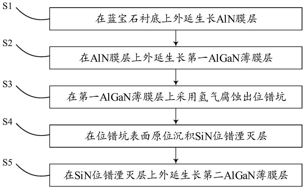
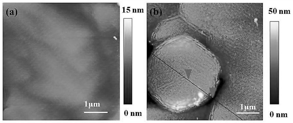
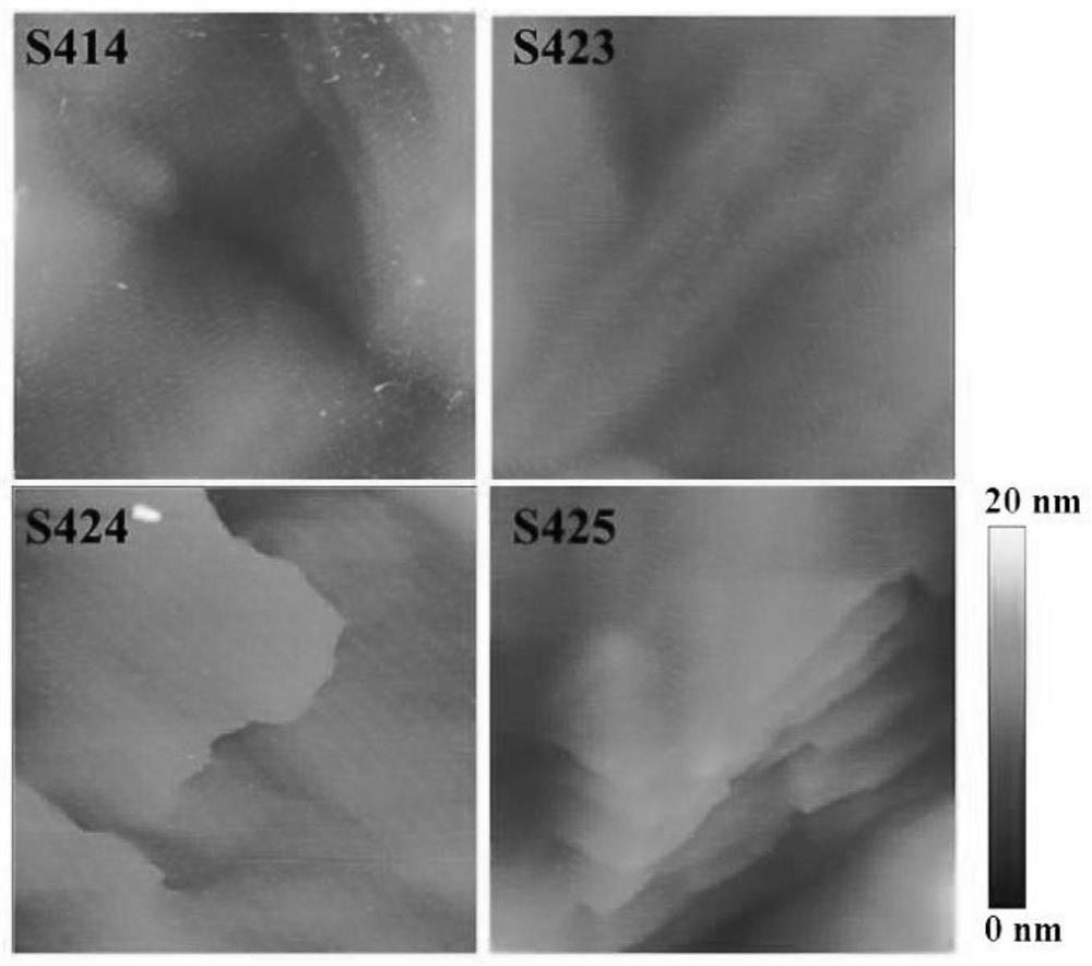
[0021] For the first solution provided by the present invention, please refer to figure 1 with figure 2 , figure 1 It is a process flow diagram of an embodiment of an epitaxial growth method of an AlGaN film with an in-situ SiN dislocation annihilation layer in the present invention, figure 2 It is a structural evolution diagram of an embodiment of an epitaxial growth method of an AlGaN thin film with an in-situ SiN dislocation annihilation layer in the present invention....


PUM

PropertyMeasurementUnit
depthaaaaaaaaaa
thicknessaaaaaaaaaa
thicknessaaaaaaaaaa

Abstract

The invention discloses an AlGaN film with an in-situ SiN dislocation annihilation layer and an epitaxial growth method thereof. The steps of the method include: epitaxially growing an AlN film on a sapphire substrate; epitaxially growing a first AlGaN thin film layer; using hydrogen gas to etch dislocation pits on the first AlGaN thin film layer; in-situ depositing a SiN dislocation annihilation layer on the surface of the dislocation pit; epitaxially growing a second dislocation annihilation layer on the SiN dislocation annihilation layer AlGaN thin film layer. In the present invention, by corroding dislocation pits on the first AlGaN thin film layer and then performing SiN in-situ filling, on the one hand, the second AlGaN thin film layer and subsequent film layers can be patterned synchronously during the growth process, It avoids the problem of taking out the epitaxial wafer for complex etching process and introducing impurities during taking out the etching; on the other hand, since the SiN dislocation annihilation layer is an island-like distribution structure corresponding to the dislocation pit, this structure is more conducive to Growth healing of the second AlGaN film layer.

Description

technical field [0001] The invention relates to the field of semiconductor optoelectronics, in particular to an AlGaN film with an in-situ SiN dislocation annihilation layer and an epitaxial growth method thereof. Background technique [0002] At present, AlGaN, as one of the important representatives of the third-generation new wide-bandgap semiconductor materials, has the characteristics of wide direct bandgap, high breakdown voltage, large electron saturation velocity, high temperature resistance, and radiation resistance, so AlGaN materials and low The three-dimensional quantum structure has incomparable advantages over traditional semiconductor materials in the production of ultraviolet detectors, ultraviolet LEDs, ultraviolet-infrared two-color detector devices and high-frequency microwave power devices, and has important applications in the fields of optoelectronics industry, biomedical industry, and national defense industry. The prospect is the key basic material to...

Claims


Application Information

Patent Timeline
Patent Type & Authority Patents(China)
IPC IPC(8): H01L33/00H01L33/20
CPCH01L33/007H01L33/20Y02P70/50
Inventor 张骏岳金顺梁仁瓅
Owner SUZHOU UVCANTEK CO LTD
Why Eureka
Try Eureka