A kind of deep ultraviolet LED with hole accumulation structure and preparation method thereof

A deep ultraviolet and hole technology, applied in semiconductor devices, electrical components, circuits, etc., can solve the problems of low luminous efficiency of deep ultraviolet LEDs, and achieve high equivalent barrier height, luminous efficiency, and hole concentration. Effect

Active Publication Date: 2022-01-28
SUZHOU UVCANTEK CO LTD
View PDF14 Cites 0 Cited by
  • Summary
  • Abstract
  • Description
  • Claims
  • Application Information

AI Technical Summary

Problems solved by technology

[0005] The object of the present invention is to provide a deep ultraviolet LED with a hole accumulation structure and its preparation method, which is used to solve the low luminous efficiency of the deep ultraviolet LED caused by the electron overflow effect and the blocking effect of the electron blocking layer in the prior art The problem

Method used


Image

  • A kind of deep ultraviolet LED with hole accumulation structure and preparation method thereof
  • A kind of deep ultraviolet LED with hole accumulation structure and preparation method thereof
  • A kind of deep ultraviolet LED with hole accumulation structure and preparation method thereof

Examples


preparation example Construction

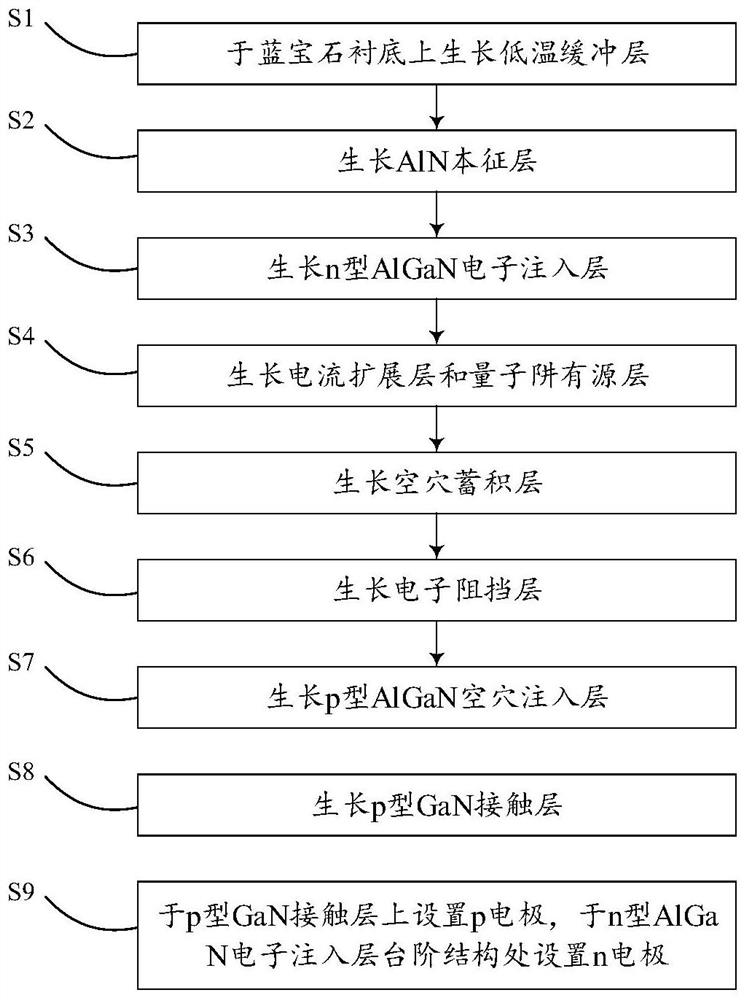
[0027] For a second solution provided by the present invention, see figure 2 , figure 2 It is a process flow chart of an embodiment of the preparation method of a deep ultraviolet LED with a hole accumulation structure in the present invention. In the present invention, the method for preparing a deep ultraviolet LED with a hole accumulation structure is used to prepare the deep ultraviolet LED with a hole accumulation structure in the aforementioned first solution, and the steps include:

[0028] S1. Under the condition of 400-800° C., grow a low-temperature buffer layer in the AlN intrinsic layer on a sapphire substrate with a thickness of 10-50 nm.

[0029] S2. The temperature is raised to 1200-1400° C., and the AlN intrinsic layer is grown on the buffer layer in the AlN intrinsic layer. The total thickness of the AlN intrinsic layer is 500-4000 nm.

[0030] S3. The temperature is lowered to 800-1200° C., and an n-type AlGaN electron injection layer is grown on the AlN ...

Embodiment 1

[0043] In this embodiment, the preparation process of the deep ultraviolet LED with the hole accumulation structure is as follows:

[0044] S1. Under the condition of 650° C., a low-temperature buffer layer in the AlN intrinsic layer is grown on a sapphire substrate with a thickness of 10 nm.

[0045] S2. The temperature is raised to 1300° C., and an intrinsic AlN layer is grown on the buffer layer in the intrinsic AlN layer. The total thickness of the intrinsic AlN layer is 2 μm.

[0046] S3. The temperature is lowered to 1050° C., and an n-type AlGaN electron injection layer is grown on the AlN intrinsic layer with a thickness of 1 μm. In this embodiment, the specific compositions of the AlN intrinsic layer and the n-type AlGaN electron injection layer are both n-type Al 0.55 Ga 0.45 N, with a total thickness of 3 μm.

[0047] S4. Lower the temperature to 1000°C, and grow a current spreading layer and a quantum well active layer sequentially on the n-type AlGaN electron i...


PUM

PropertyMeasurementUnit
thicknessaaaaaaaaaa
thicknessaaaaaaaaaa
thicknessaaaaaaaaaa

Abstract

The invention discloses a deep ultraviolet LED with a hole accumulation structure and a preparation method thereof. The deep ultraviolet LED with a hole accumulation structure is sequentially provided with a sapphire substrate, an AlN intrinsic layer, and an n-type AlGaN electron Injection layer, current spreading layer, quantum well active layer, hole storage layer, electron blocking layer, p-type AlGaN hole injection layer and p-type GaN contact layer; the hole storage layer is Mg-doped single-layer AlGaN structure, the growth temperature is 600-1000°C. The present invention increases the hole accumulation layer of single-layer structure between the quantum well active layer and the electron blocking layer, while increasing the equivalent potential barrier height of the electron blocking layer, and increasing the holes injected into the quantum well active region Concentration, and ultimately improve the luminous efficiency of deep ultraviolet LED devices.

Description

technical field [0001] The invention relates to the field of semiconductor optoelectronics, in particular to a deep ultraviolet LED with a hole storage structure and a preparation method thereof. Background technique [0002] At present, group III nitrides, as outstanding representatives of wide bandgap semiconductor materials, have realized high-efficiency blue-green light-emitting diodes (light-emitting diodes, LEDs), lasers and other solid-state light source devices, which are used in flat panel displays, white lighting and other applications. achieved great success. In the past ten years, people expect to apply this high-efficiency luminescent material to the ultraviolet band to meet the increasing demand for ultraviolet light sources. According to its biological effects, the ultraviolet band can usually be divided into: long-wave ultraviolet (UVA, 320nm-400nm), medium-wave ultraviolet (UVB, 280nm-320nm), short-wave ultraviolet (UVC, 200nm-280nm) and vacuum ultraviolet ...

Claims


Application Information

Patent Timeline
Patent Type & Authority Patents(China)
IPC IPC(8): H01L33/14H01L33/00
CPCH01L33/14H01L33/007
Inventor 张骏岳金顺梁仁瓅
Owner SUZHOU UVCANTEK CO LTD
Why Eureka
Try Eureka