

Optical imaging lens and imaging equipment
An optical imaging lens and imaging surface technology, applied in the field of imaging lenses, can solve the problems of high manufacturing cost and poor market competitiveness, and achieve the effects of low cost, correction of thermal focal shift, and weight reduction of the lens
- Summary
- Abstract
- Description
- Claims
- Application Information
AI Technical Summary
Problems solved by technology
Method used
Image

Examples
no. 1 example
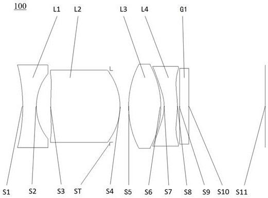
[0054] see figure 1 , which is a schematic structural view of the optical imaging lens 100 provided in the first embodiment of the present invention, the optical imaging lens 100 includes in sequence from the object side to the imaging surface along the optical axis: a first lens L1, a second lens L2, and a stop ST , the third lens L3, the fourth lens L4, the filter G1 and the imaging surface S11.
[0055] Wherein, the first lens L1 has negative refractive power, the object side S1 of the first lens L1 is a concave surface, and the image side S2 of the first lens L1 is a concave surface;
[0056] The second lens L2 has positive refractive power, the object side S3 of the second lens L2 is a convex surface, and the image side S4 of the second lens L2 is a convex surface;
[0057] The third lens L3 has positive refractive power, the object side S5 of the third lens L3 is a convex surface, and the image side S6 of the third lens L3 is a convex surface;
[0058] The fourth lens ...
no. 2 example
[0071] The structure of the optical imaging lens provided by the second embodiment of the present invention is substantially the same as that of the optical imaging lens 100 in the first embodiment, except that the relevant parameters such as the radius of curvature, thickness, and material of each lens are different.
[0072] The relevant parameters such as the radius of curvature, thickness, and material of each lens of the optical imaging lens in this embodiment are shown in Table 3.
[0073] table 3
[0074]
[0075] The surface coefficients of each aspheric surface of the optical imaging lens in this embodiment are shown in Table 4.
[0076] Table 4
[0077]
[0078] see Figure 4 , shows the field curvature curve of the optical imaging lens in this embodiment. It can be seen from the figure that the field curvature of the meridian image plane and the sagittal image plane is controlled within ±0.12mm, indicating that the field curvature correction of the optical ...
no. 3 example
[0081] The structure of the optical imaging lens provided by the third embodiment of the present invention is substantially the same as that of the optical imaging lens 100 in the first embodiment, except that the curvature radius, thickness, material and other related parameters of each lens are different.
[0082] The relevant parameters such as the radius of curvature, thickness, and material of each lens of the optical imaging lens in this embodiment are shown in Table 5.
[0083] table 5
[0084]
[0085] The surface coefficients of each aspheric surface of the optical imaging lens in this embodiment are shown in Table 6.
[0086] Table 6
[0087]
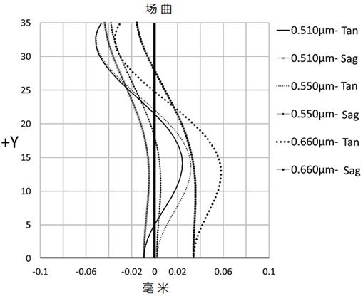
[0088] see Image 6 , shows the field curvature curve of the optical imaging lens in this embodiment. It can be seen from the figure that the field curvature of the meridian image plane and the sagittal image plane is controlled within ±0.06mm, indicating that the field curvature correction of the optical imaging lens...
PUM
 Abstract
Description
Claims
Application Information