A low-power LED lamp bead low thermal resistance packaging structure and packaging process
A technology of LED lamp beads and packaging structure, applied in the direction of semiconductor devices, electrical components, circuits, etc., can solve the problems of low degree of automation of dam and sealing process, great influence of phosphor attenuation, and decreased phosphor conversion efficiency, etc. Achieve the effect of easy defoaming, increase high refractive index and high light transmittance, and facilitate disassembly
- Summary
- Abstract
- Description
- Claims
- Application Information
AI Technical Summary
Problems solved by technology
Method used
Image
Examples
Embodiment 1
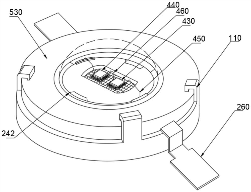
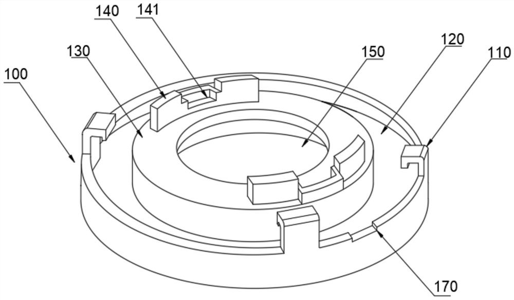
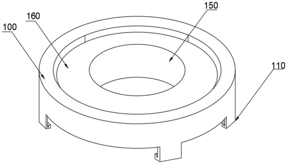
[0049] Embodiment 1, with reference to attached Figure 1-15 , a low thermal resistance packaging structure for low-power LED lamp beads provided by the present invention, including a base 100, a support base 200, a heat conduction device 300, a light-emitting component 400, an insulating sleeve 500 and a protection component 600, and the top of the base 100 is provided with a mounting groove 120 Specifically, the inner wall of the installation groove one 120 is provided with a support seat 200, the support seat 200 includes a chassis 210, the top of the chassis 210 is fixedly installed with a boss two 220, and the top of the boss two 220 is fixedly installed with a pad seat 230, and the pad seat 230 The top is provided with a cutting surface 232, the pad seat 230 is provided with a slot one 231 on both sides, and the inner wall of the slot one 231 is plugged with an electrode pin 260, and one end of the electrode pin 260 is fixedly installed on the inner wall of the cutting su...
Embodiment 2
[0061] A low-power LED lamp bead packaging process with low thermal resistance, the operating steps are:
[0062] Step 1: Ultrasonic cleaning of base 100, support base 200, heat conduction device 300 and insulating sleeve 500, and drying to remove moisture;
[0063] Step 2: Insert the chassis 210 into the inner wall of the installation slot 120, rotate the support base 200 so that the bump 140 and the groove 141 are clamped on the inner wall of the slot 2 250 and the bump 3 251, insert the pad 310 and the copper pillar 320 On the inner wall of the through hole 240, the pad 310 is installed on the top of the retaining ring 241, adjust the position of the pad 310 so that the groove 2 312 is engaged with the bump 242, and insert one end of the two sets of electrode pins 260 into the inner wall of the slot 1 231 , fixed at the connection between the cut surface 232 and the pad 310, and the bottom end of the electrode pin 260 is installed in the slot two 270 and the slot one 170 fo...
Embodiment 3
[0071] Refer to the attached Figure 16 , a low thermal resistance packaging structure of a low-power LED lamp bead in this embodiment, further comprising an aluminum column 370;
[0072] Further, the bottom of the copper column 320 is provided with a mounting groove 321, and the inner wall of the mounting groove 321 is fixed with an aluminum column 370. Specifically, the mounting groove 321 has a limiting effect on the aluminum column 370, and the aluminum column 370 has a positioning effect on the copper column 320. The effect of heat conduction efficiency and heat dissipation, the aluminum column 370 has good thermal conductivity and is not easy to rust and has the effect of reducing production cost.
[0073] The specific implementation scenario is: when using the present invention, workers in the field need to replace the aluminum pillars 370 with copper pillars 320 .
PUM
 Abstract
Description
Claims
Application Information


