

Power semiconductor device and preparation method thereof
A technology of power semiconductors and devices, which is applied in the field of power semiconductor devices and their preparation, and can solve problems affecting the avalanche tolerance of devices
- Summary
- Abstract
- Description
- Claims
- Application Information
AI Technical Summary
Problems solved by technology
Method used
Image

Examples
Embodiment 1
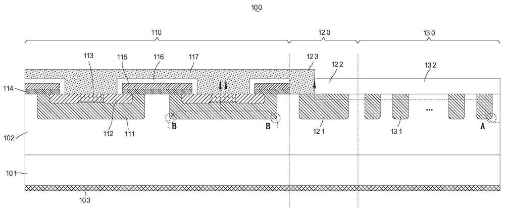
[0053] Such as Figure 4 As shown, the embodiment of the present disclosure provides a power semiconductor device 200 , including a substrate 201 , an epitaxial layer 202 , a drain metal layer 203 , an active region 210 , a transition region 220 and a terminal region 230 .
[0054] Exemplarily, the substrate 201 is a silicon carbide substrate or a silicon substrate of the first conductivity type. The resistivity of the substrate 201 is 0.01 to 0.03 Ω·cm, and the thickness is 200 to 400 μm.
[0055] The epitaxial layer 202 is an epitaxial layer of the first conductivity type and is located above the substrate 201 . The ion doping concentration of the epitaxial layer 202 is 5e14 to 5e16 cm -3 . The doping concentration and thickness of the epitaxial layer 202 are adjusted according to different device withstand voltage capabilities.
[0056] The drain metal layer 203 is located under the substrate 201 and forms an ohmic contact with the substrate 201 .
[0057] The active r...
Embodiment 2
[0078] On the basis of the first embodiment, this embodiment provides a method for manufacturing a power semiconductor device 200 . Figure 6 It is a schematic flowchart of a manufacturing method of a power semiconductor device 200 shown in an embodiment of the present disclosure. Figure 7-Figure 12 It is a schematic cross-sectional structure formed by related steps of a method for manufacturing a power semiconductor device 200 shown in an embodiment of the present disclosure. Below, refer to Figure 6 and Figure 7-Figure 12 The detailed steps of an exemplary method of the method for manufacturing the power semiconductor device 200 proposed by the embodiment of the present disclosure will be described.
[0079] Such as Figure 6 As shown, the manufacturing method of the power semiconductor device 200 in this embodiment includes the following steps:
[0080] Step S101 : providing a first conductivity type substrate 201 .
PUM
 Abstract
Description
Claims
Application Information