Organic light-emitting device, preparation method and display panel

A technology of organic light-emitting devices and fluorescent dopants, which is applied in the direction of organic semiconductor devices, semiconductor/solid-state device manufacturing, electric solid-state devices, etc., can solve problems such as hindering development, efficiency roll-off, etc., to improve efficiency and reduce efficiency roll-off , Improve the effect of exciton utilization

Pending Publication Date: 2021-01-26
BOE TECH GRP CO LTD +1
View PDF0 Cites 1 Cited by
  • Summary
  • Abstract
  • Description
  • Claims
  • Application Information

AI Technical Summary

Problems solved by technology

At present, TADF-type interfacial exciplexes still face serious efficiency roll-off problems, hindering their development.

Method used


Image

  • Organic light-emitting device, preparation method and display panel
  • Organic light-emitting device, preparation method and display panel
  • Organic light-emitting device, preparation method and display panel

Examples


preparation example Construction

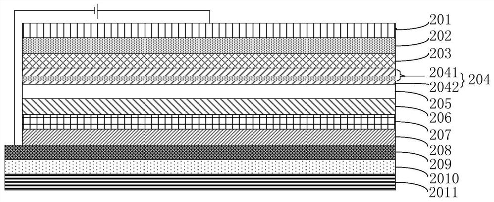
[0138] In the second aspect of the present specification, a method for preparing an organic light-emitting device is also provided. see Figure 5 , the preparation method comprises the steps of:

[0139] Step 501: Provide a substrate.

[0140] It should be noted that the substrate includes an anode and a hole transport layer.

[0141] It should be noted that the anode is disposed on the BP substrate. Optionally, the BP substrate is ultrasonically cleaned in acetone, ethanol and deionized water in sequence, and then dried in an oven for use.

[0142] Optionally, the anode is substantially prepared by sputtering an anode material onto the BP in a vacuum chamber.

[0143] Optionally, the hole transport layer is prepared by vacuum evaporation.

[0144] In some optional embodiments, the substrate further includes a hole injection layer, and the hole injection layer is located between the hole transport layer and the anode. Optionally, the hole injection layer is prepared by e...

Embodiment 1

[0175] Example 1: Top emission doped organic light emitting device

[0176] The specific structure is as follows: ITO / HIL (10nm) / HTL (90nm) / p-type matrix material (15nm)+p-type matrix material (20nm): FD (10%)+p-type matrix material (5nm) / Interlayer (x nm ) / n-type host material (40nm) / ETL (50nm) / EIL (3nm) / Mg:Ag. Here, x represents the thickness of Interlayer. Wherein, x=1 nm, 4 nm or 8 nm.

Embodiment 2

[0177] Example 2: Top emission doped organic light emitting device

[0178] The specific structure is as follows: ITO / HIL (10nm) / HTL (90nm) / p-type matrix material (40nm) / Interlayer (xnm) / n-type matrix material (5nm)+n-type matrix material (20nm):FD (10%) +n-type host material (15nm) / ETL (50nm) / EIL (3nm) / Mg:Ag. Here, x represents the thickness of Interlayer. Wherein, x=1nm, 4nm, 8nm.


PUM

PropertyMeasurementUnit
Thicknessaaaaaaaaaa
Thicknessaaaaaaaaaa
Thicknessaaaaaaaaaa

Abstract

The embodiment of the invention provides an organic light-emitting device, a preparation method and a display panel. Specifically, the organic light-emitting device comprises a p-type host layer, an n-type host layer and an intermediate layer located between the p-type host layer and the n-type host layer, wherein at least one of the p-type substrate layer and the n-type substrate layer is provided with a fluorescent dopant, and the fluorescent dopant is close to the intermediate layer and has a preset distance from the intermediate layer; the p-type matrix layer and the n-type matrix layer are configured to form a spatially separated exciplex with the intermediate layer under the action of electricity; and the fluorescent dopant is configured to obtain the energy of singlet excitons generated by the exciplex and emit light. According to the technical scheme, the distribution area of excitons formed by the exciplex can be enlarged, and exciton quenching and efficiency roll-off caused by excessive concentration of the excitons are effectively reduced.

Description

technical field [0001] The embodiments of this specification relate to the technical field of organic electroluminescence display, and in particular to an organic light emitting device, a manufacturing method and a display panel. Background technique [0002] Thermally-Activated Delayed Fluorescence (TADF) technology, as an OLED technology with application potential, has achieved rapid development in recent years and is known as the third-generation OLED technology. Among them, the TADF-type interface exciton complex (n-type + p-type) as the host (Host) is the focus of the development of the third-generation OLED technology. This technology collects ~100% of the singlet excitons (S1) through the delayed fluorescence effect and transmits them. Give the dopant a theoretical breakthrough in the IQE value. At present, TADF-type interfacial exciplexes still face a serious efficiency roll-off problem, which hinders their development. Contents of the invention [0003] In view ...

Claims


Application Information

Patent Timeline
IPC IPC(8): H01L51/50H01L51/56H01L27/32
CPCH10K59/10H10K50/11H10K2101/40H10K50/12H10K71/00H10K50/121H10K2101/30H10K2102/351
Inventor 杨绘耘张晓晋孙海雁
Owner BOE TECH GRP CO LTD
Why Eureka
Try Eureka