Inverted GaN power device packaging structure and preparation method thereof

A technology of power devices and packaging structures, applied in the field of manufacturing

Active Publication Date: 2021-01-29
JIANGSU JIEJIE MICROELECTRONICS
View PDF5 Cites 0 Cited by
  • Summary
  • Abstract
  • Description
  • Claims
  • Application Information

AI Technical Summary

Problems solved by technology

[0003] In order to solve the problem of reducing the stray inductance caused by bonding wires, the present invention discloses a package structure of a flip-chip GaN power device and a preparation method thereof

Method used


Image

  • Inverted GaN power device packaging structure and preparation method thereof
  • Inverted GaN power device packaging structure and preparation method thereof
  • Inverted GaN power device packaging structure and preparation method thereof

Examples


Embodiment Construction

[0025] In order to deepen the understanding of the present invention, the specific implementation of the present invention will be described in detail below in conjunction with the accompanying drawings. This embodiment is only used to explain the present invention and does not constitute a limitation to the protection scope of the present invention.

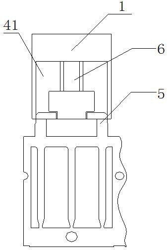
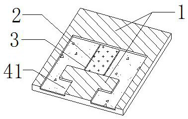
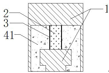
[0026] Such as Figure 1-8 As shown, a flip-chip GaN power device packaging structure includes a ceramic substrate 1. The ceramic substrate 1 has a rectangular shape and a material thickness of 1mm. The shape of the body is inverted "concave". The bottom of the slotted tank and the back of the ceramic substrate are respectively covered with a front copper layer 41 and a rear copper layer 42. The thickness of the copper layer is 0.15mm. The upper middle of the inverted "concave" tank is coated with There is insulating varnish 2, the thickness of insulating varnish 2 is 0.015mm, there is a V groove 3 between the two sides of the l...


PUM


Abstract

The invention discloses an inverted GaN power device packaging structure, which comprises a ceramic substrate, an open groove is formed in the surface of the ceramic substrate in a sinking mode, a groove body of the open groove is in an inverted concave shape, and the bottom of the groove body of the open groove and the back of the ceramic substrate are covered with copper layers. The middle of the upper portion of the inverted concave shaped groove body is coated with insulating paint, V-shaped grooves are formed between the two sides of the long edges of the insulating paint layer and the front copper layer, soldering paste is applied to the lower portion and the front copper layer on one side of the long edge of the inverted concave shaped groove body, and a chip is attached to one sideof the front copper layer, far from the insulating paint, on the outer side of each V-shaped groove through soldering paste. The lower portion of the inverted concave shaped groove body is welded toa lead frame foot stand welding area through soldering paste, it is guaranteed that a chip is safely welded in an inverted-buckling state, the lead frame is positioned, and it is guaranteed that the frame does not slip in the welding process.

Description

technical field [0001] The invention relates to the field of manufacturing, in particular to a packaging structure of a flip-chip GaN power device and a preparation method thereof. Background technique [0002] The existing common chip mounting process uses solder paste as an adhesive to mount the backside of the chip on the chip loading area of ​​the lead frame. At the same time, in order to achieve the effect of forming an electrical connection between the chip and the pins of the device, wire bonding or copper bridging is often used between the active area on the front of the chip and the pins. This process method has been widely used and recognized by the industry, and has reliable operability. However, the bonding wire (or copper bridge) will generate stray inductance in the entire electrical circuit, and high-frequency devices are particularly sensitive to stray inductance. As the stray inductance increases, the turn-on loss increases. Stray inductance can also cause...

Claims


Application Information

Patent Timeline
Patent Type & Authority Applications(China)
IPC IPC(8): H01L23/14H01L23/488H01L23/495H01L21/58H01L29/861H01L29/20
CPCH01L23/14H01L23/488H01L23/495H01L21/50H01L29/861H01L29/2003
Inventor 王其龙徐洋施嘉颖杨凯锋顾红霞
Owner JIANGSU JIEJIE MICROELECTRONICS
Why Eureka
Try Eureka