Sensitization method for PbS thin film, infrared photoelectric detector and preparation method thereof

An electrical detector, infrared light technology, applied in semiconductor/solid-state device manufacturing, circuits, electrical components, etc., can solve the problems of low sensitivity of infrared photodetectors, unsatisfactory sensitization effect, complex operation process, etc., to eliminate Potential safety hazards, short response time, low sensitization temperature effects

Active Publication Date: 2021-02-02
HUNAN UNIV
View PDF7 Cites 0 Cited by
  • Summary
  • Abstract
  • Description
  • Claims
  • Application Information

AI Technical Summary

Problems solved by technology

It can be seen that the existing PbS thin film sensitization method still has complex operation process, high sensitization temperature, high energy consumption, high temperature resistant substrate material, unsatisfactory sensitization effect, and infrared photodetection based on PbS photoresistor. The sensitivity of the sensor is not high, which greatly limits its application in the field of gas detection.

Method used


Image

  • Sensitization method for PbS thin film, infrared photoelectric detector and preparation method thereof
  • Sensitization method for PbS thin film, infrared photoelectric detector and preparation method thereof
  • Sensitization method for PbS thin film, infrared photoelectric detector and preparation method thereof

Examples


preparation example Construction

[0050] The preparation method of the near-infrared photodetector based on PbS thin film of the present invention, comprises the steps:

[0051] S1: PbS thin film is prepared on conductive glass or silicon wafer substrate.

[0052] Specifically, the PbS thin film can be prepared by chemical water bath deposition method, and its thickness is 500-700nm. In addition, PbS thin films can also be prepared by magnetron sputtering and ion beam sputtering. When prepared by chemical water bath deposition method, the process is as follows:

[0053] Fully clean the ITO transparent conductive glass, store it in a petri dish, and put the petri dish into an oven to dry for later use.

[0054] Weigh NaOH, CS(NH 2 ) 2 , Pb(NO 3 ) 2 And prepare NaOH concentration to be 0.1M (mol / L), CS (NH 2 ) 2 The concentration is 60mM(mmol / L), Pb(NO 3 ) 2 A solution with a concentration of 9mM (mmol / L). Slowly add Pb(NO 3 ) 2 Solution, continue to stir until the solution is transparent, soak the ...

Embodiment 1

[0067] The invention provides a kind of preparation method based on the near-infrared photodetector of PbS film, comprises the steps:

[0068] S1: A PbS thin film is prepared on an ITO conductive glass substrate, the process is as follows:

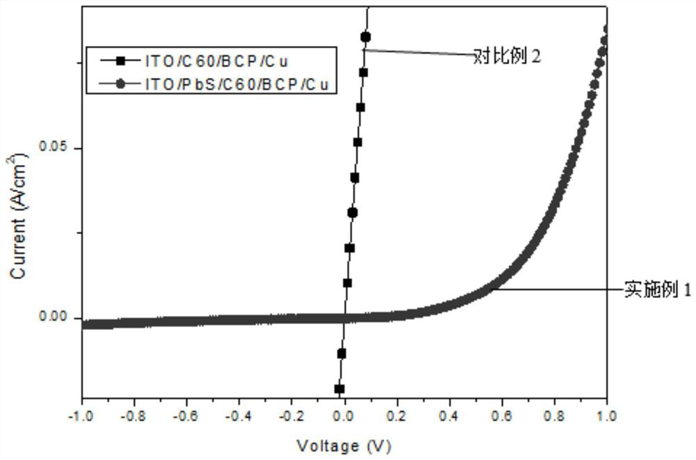
[0069] Take a piece of ITO transparent conductive glass with a size of 14.9mmx10mm, a thickness of about 135nm, a square resistance of less than 15 ohms, and a transmittance greater than 86%. First soak the ITO transparent conductive glass in deionized water and put it in an ultrasonic cleaner for 10 minutes. minutes, repeat the operation twice. Then ultrasonically clean the ITO transparent conductive glass bubbles in acetone for 10 minutes, and repeat twice. Finally, ultrasonically clean the ITO transparent conductive glass bubbles in isopropanol for 10 minutes / time, twice. The cleaned ITO transparent conductive glass is taken out and stored in a petri dish, and the petri dish is put into an oven to dry for later use.

[0070] Weigh Na...

Embodiment 2

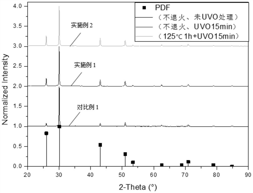
[0076] The difference between Example 2 and Example 1 is that after the PbS film is prepared on the ITO transparent conductive glass in step S1, the PbS film is annealed in air at 125° C. for 1 h to promote the growth of PbS crystal grains, and then according to Example The steps, methods and conditions of S2-S5 in 1 are processed in the same way. After the treatment, the microscopic morphology of the PbS thin film is as follows: Figure 5 shown. It can be seen from the figure that the PbS grain size at this time is uniform, the grain size is large, and the crystallinity is good.


PUM

PropertyMeasurementUnit
thicknessaaaaaaaaaa
thicknessaaaaaaaaaa
thicknessaaaaaaaaaa

Abstract

The invention relates to a novel sensitization method for a PbS thin film. According to the method, ultraviolet ozone treatment is carried out on the PbS thin film to sensitize the PbS thin film. Theinvention also relates to an infrared photoelectric detector based on the PbS film and a preparation method. The detector comprises a conductive glass or silicon wafer substrate layer, a p-type semiconductor layer, an n-type semiconductor layer, a buffer layer and an electrode layer. The p-type semiconductor layer is a PbS thin film subjected to ultraviolet ozone sensitization treatment; and the n-type semiconductor layer is fullerene C60 or a derivative thereof. According to the method, UVO sensitization treatment is adopted, the sensitization temperature is low, energy consumption is low, operation is easy, and the sensitization effect is remarkable. In addition, the infrared photoelectric detector is a high-sensitivity infrared photoelectric detector which is provided with a diode structure and can work at room temperature, and the specific detection rate is obviously superior to that of a traditional photoresistor type detector.

Description

technical field [0001] The invention relates to the technical field of infrared detector preparation, and relates to a PbS thin film sensitization method, an infrared photodetector and a preparation method thereof. Background technique [0002] Infrared detector (Infrared Detector) is a device that converts infrared light signals into electrical signals for output. The widely used infrared photodetectors are mainly based on PbS, PbSe, Ge, InSb, HgCdTe, InGaAs and other materials. Because PbS and PbSe have low dark current characteristics under uncooled conditions, infrared photodetectors made of them can reduce noise without additional cooling equipment. The existing PbS thin film preparation methods mainly include: chemical bath deposition (CBD) method, physical vapor deposition (magnetron sputtering, high vacuum thermal evaporation deposition, etc.). [0003] In order to further reduce the dark current of PbS under uncooled conditions and improve the sensitivity to infra...

Claims


Application Information

Patent Timeline
Patent Type & Authority Applications(China)
IPC IPC(8): H01L31/18H01L31/101H01L31/0216H01L21/02
CPCH01L31/18H01L31/101H01L31/02161H01L21/02664Y02P70/50Y02E10/549
Inventor 杨斌孙景潘安练
Owner HUNAN UNIV
Why Eureka
Try Eureka