Area array point scanning light-splitting white-light interferometer

A white light interferometer and point scanning technology, applied in the field of optical instruments, can solve the problems of uneven energy, misjudgment of detection results, inability to receive reflected light, etc., and achieve the effect of good energy uniformity

Active Publication Date: 2021-02-05
SUZHOU CASIA ALL PHASE INTELLIGENCE TECH CO LTD +1
View PDF11 Cites 6 Cited by
  • Summary
  • Abstract
  • Description
  • Claims
  • Application Information

AI Technical Summary

Problems solved by technology

When the reflected light of the sample is specular reflection, the sample objective lens cannot receive enough reflected light in the off-axis field of view, and the detection effect cannot be

Method used


Image

  • Area array point scanning light-splitting white-light interferometer
  • Area array point scanning light-splitting white-light interferometer
  • Area array point scanning light-splitting white-light interferometer

Examples


Embodiment 1

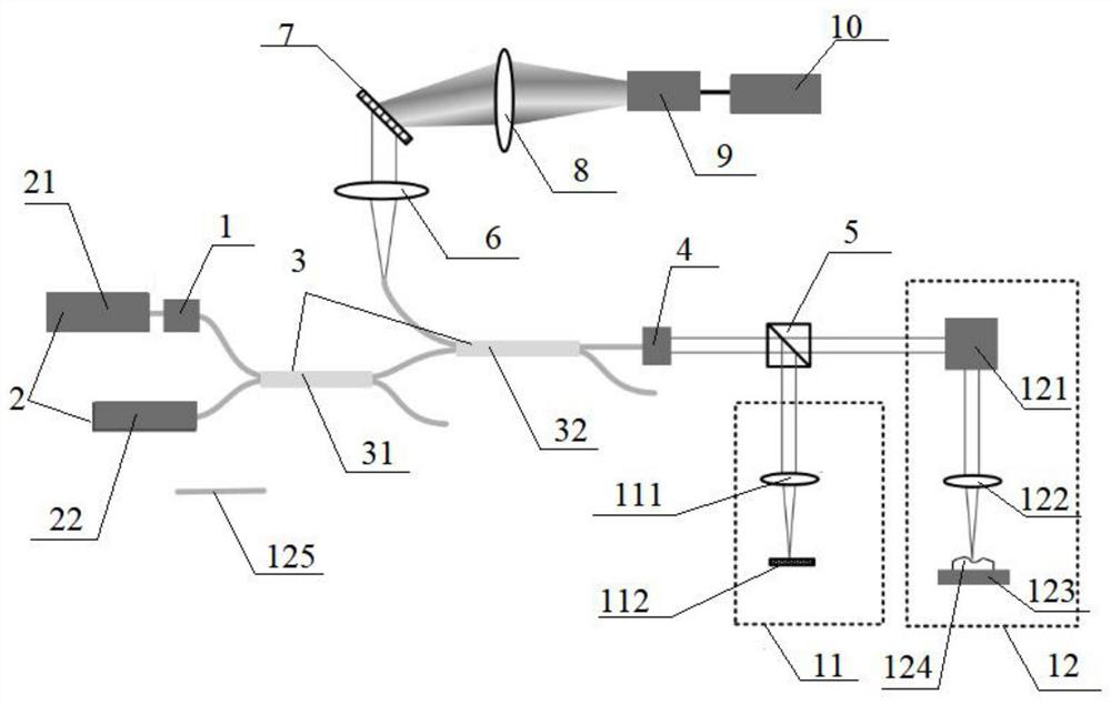
[0065] Such as Figure 1-4 As shown, the SLD light source uses a near-infrared broadband light source with a power of 25mw and a wavelength of 810-870nm; the isolator uses an 850nm broadband isolator; the coupler is an X-type single-mode fiber coupler, the numerical aperture of the fiber is 0.13, the core diameter is 5um, and the splitting ratio is 50 : 50; collimator adopts diffractive polar achromatic lens, focal length is 18.45mm; beam splitting prism splitting ratio is 50:50; third lens is achromatic lens with focal length 50mm; mirror is coated with near-infrared high reflection film, reflectivity >99.5% ;The XY scanning galvanometer has an effective incident spot diameter of 7mm and a maximum scanning angle of 5 degrees; the grating is a 1800lp transmission grating with a blaze angle of 49.2 degrees@840nm; the first lens and the second lens use the same achromatic telecentric lens, and the field of view angle is 10 degrees , the focal length is 83.9mm; the pixel size of ...

Embodiment 2

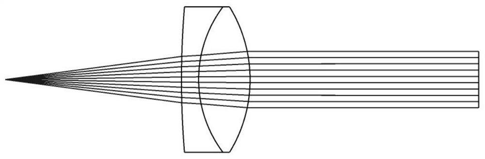
[0068] Such as Figure 10 As shown, compared with Embodiment 1, the remaining modules remain unchanged, and only the fourth lens is replaced to achieve different scanning ranges and different depths of field. The fourth lens has a field of view of 28 degrees, a focal length of 70mm, and an entrance pupil diameter of 5mm. The scanning field of view is 24.4*24.4mm, and the depth of field is 0.67mm.

[0069] Such as Figure 11 as shown, Figure 11 It is the MTF curve of the fourth lens of this embodiment, which basically reaches the diffraction limit level and has high resolution.

Embodiment 3

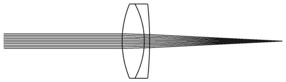
[0071] Such as Figure 12 As shown, compared with Embodiment 1, the remaining modules remain unchanged, and the fourth lens is replaced to achieve different scanning ranges and different depths of field. The fourth lens has a field of view of 28 degrees, a focal length of 100mm, and an entrance pupil diameter of 5mm. The scanning field of view is 34.9*34.9mm, and the depth of field is 1.36mm.

[0072] Such as Figure 13 as shown, Figure 13 It is the MTF curve of the fourth lens in Example 3, which basically reaches the diffraction limit level and has high resolution.


PUM

PropertyMeasurementUnit
Core diameteraaaaaaaaaa

Abstract

The invention relates to an area array point scanning light-splitting white-light interferometer. An SLD light source emits a broadband spectrum, light sequentially passes through an isolator and an optical fiber coupler, an optical fiber end emits emergent light that is collimated through a collimator and is incident to a beam splitter prism by the collimated light, one beam of light is reflectedand focused to a reflector through a third lens to serve as a reference arm, and the other beam of light is incident to an XY scanning galvanometer; light with a certain field angle is reflected by ascanning galvanometer and enters a fourth lens, and the light is focused to a sample through the fourth lens to achieve area array scanning. The XY scanning galvanometer is placed at the object spacefocal plane position of the fourth lens, so that the focusing light of the fourth lens is an image space telecentric light path; area array scanning can be realized in a high-speed, concise and high-precision manner.

Description

technical field [0001] The invention relates to an optical instrument, in particular to an optical instrument for non-contact measurement, and more particularly to an area array point scanning spectroscopic white light interferometer. Background technique [0002] The white light scanning interference technology uses white light as the light source, its coherence length is short, and the interference fringes only appear in a small range. When the optical path difference is zero, the interference signal has a maximum value, and this point represents the height information of the corresponding point, which can Restore the overall shape of the tested sample. Spectroscopic white light interferometer is an important direction of white light interference. This technology mainly uses spectrometers for collection, splits white light into different wavelengths, and determines surface morphology by analyzing spectral signals. Compared with traditional white light interferometry techno...

Claims


Application Information

Patent Timeline
IPC IPC(8): G01B9/02
CPCG01B9/02
Inventor 赵效楠王毅彭思龙汪雪林顾庆毅王一洁
Owner SUZHOU CASIA ALL PHASE INTELLIGENCE TECH CO LTD
Why Eureka
Try Eureka