Output stage circuit of high-side power switch

An output stage circuit and power switch technology, applied in circuits, electronic switches, electrical components, etc., can solve the problems of large layout area and high power consumption, and achieve the effect of avoiding burnout and reducing layout area and power consumption.

Active Publication Date: 2021-02-09
UNIV OF ELECTRONICS SCI & TECH OF CHINA
View PDF10 Cites 6 Cited by
  • Summary
  • Abstract
  • Description
  • Claims
  • Application Information

AI Technical Summary

Problems solved by technology

[0005] Aiming at the shortcomings of large layout area and high power consumption in the solution of the high-side power switch output stage circuit in the traditional intelligent power switch for the rapid demagnetization of the inductive load, the present invention proposes an output stage circuit of the high-side power switch, which is suitable for The high-side power switch in the smart power switch chip uses the first PMOS transistor MP1 to charge the gate of the high-side power transistor during the demagnetization process of the inductive load, and turns on the high-side power transistor again to realize the function of fast demagnetization. The layout area and power consumption are reduced; in addition, the gate protection and current limiting functions are proposed to protect the safe operation of the high-side power tube while normally driving the high-side power tube switch

Method used


Image

  • Output stage circuit of high-side power switch
  • Output stage circuit of high-side power switch
  • Output stage circuit of high-side power switch

Examples


Embodiment Construction

[0025] The technical solution of the present invention will be described in detail below in conjunction with the accompanying drawings and specific embodiments.

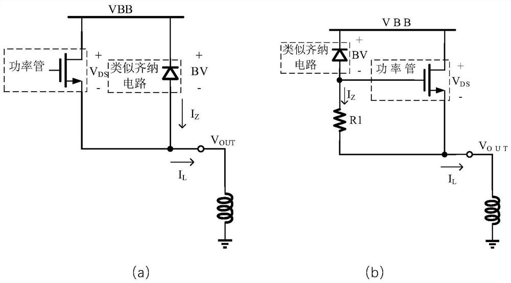
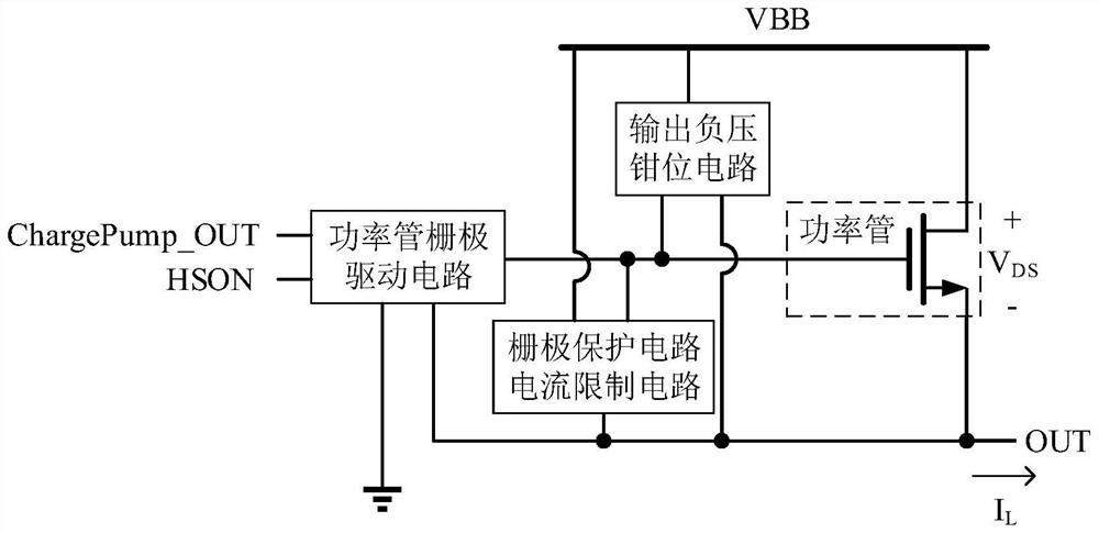
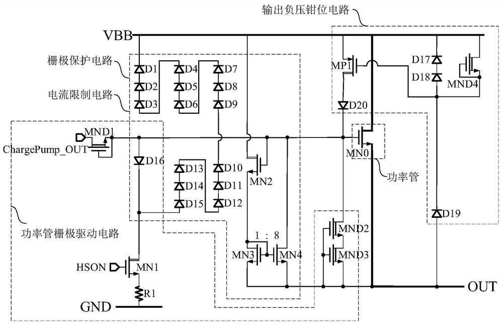
[0026] The present invention proposes an output stage circuit of a high-side power switch, including a high-side power transistor MN0, a power transistor gate drive module, and an output negative pressure clamping module, wherein the high-side power transistor MN0 is an NMOS power transistor, and its drain is connected to The source of the power supply voltage VBB is used as the output terminal OUT, and the output terminal OUT is also the output terminal of the intelligent power switch chip.

[0027] The power transistor gate drive module is used to drive and control the high-side power transistor MN0. When it is necessary to drive the high-side power transistor MN0 to be turned on, the power transistor gate driver module charges the gate of the high-side power transistor MN0 to turn on the high-side power tube MN0; ...


PUM


Abstract

The invention discloses an output stage circuit of a high-side power switch, and belongs to the technical field of power integrated circuits. According to the invention, the high-side power tube is driven and controlled by the power tube grid driving module, the design of the output negative voltage clamping module is combined to realize inductive load rapid demagnetization and rising slope control, when the inductive load is demagnetized, a seventeenth diode, an eighteenth diode and a nineteenth diode in the output negative voltage clamping module are broken down. The first PMOS tube is opened to charge the grid electrode of the high-side power tube, so that the high-side power tube is rapidly opened, the voltage of the output node is prevented from further dropping, the voltage clampingof the output node is realized, and the layout area and the power consumption are reduced compared with the traditional inductive load rapid demagnetization scheme; meanwhile, the grid protection module and the current limiting module are designed, so that the output stage circuit can limit the maximum current of the high-side power tube while normally driving the high-side power tube to be switched on and off, and the high-side power tube is prevented from being burnt out.

Description

technical field [0001] The invention belongs to the technical field of power integrated circuits and relates to an output stage circuit of a high-side power switch. Background technique [0002] An intelligent power switch refers to an integrated circuit that integrates drive circuits, diagnostic circuits, protection circuits, peripheral interface circuits, and power devices into one chip. It has a wide range of applications in automotive electronics and avionics. It can drive wipers, fuel injectors and other equipment in automobiles. It can be used in discrete output interface circuits in avionics systems. The above application scenarios all have the characteristics of harsh working environment and complex load types. Therefore, the high-side power switch output stage circuit in the smart power switch needs to have the ability to protect the power tube gate oxide layer from breakdown, make the inductive load demagnetize quickly, limit the The function of the maximum curren...

Claims


Application Information

Patent Timeline
Patent Type & Authority Applications(China)
IPC IPC(8): H03K17/687H03K17/081H03K17/082
CPCH03K17/687H03K17/6871H03K17/0822H03K17/08104Y02B70/10
Inventor 甄少伟梁怀天方舟罗攀易子皓张波
Owner UNIV OF ELECTRONICS SCI & TECH OF CHINA
Why Eureka
Try Eureka