Unimolecular transistor

A transistor and single-molecule technology, applied in transistors, electric solid-state devices, semiconductor devices, etc., can solve problems such as upper limit of working speed, increased power consumption, and increased cut-off leakage current

Pending Publication Date: 2021-02-19
JAPAN SCI & TECH CORP
View PDF0 Cites 0 Cited by
  • Summary
  • Abstract
  • Description
  • Claims
  • Application Information

AI Technical Summary

Problems solved by technology

However, with the miniaturization, several problems also emerged
For example, various problems have been pointed out: increase of off-leakage current due to short-channel effect of transistors, increase of gate leakage current d

Method used


Image

  • Unimolecular transistor
  • Unimolecular transistor
  • Unimolecular transistor

Examples


Embodiment 1

[0163] 4 Manufacturing Example of Single Molecular Transistor

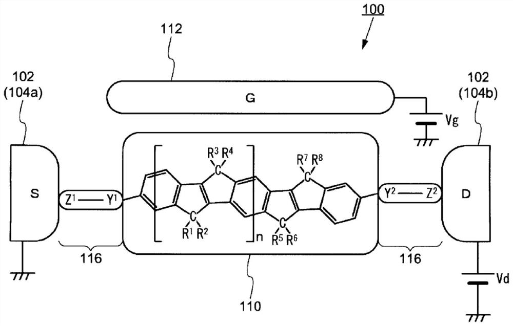
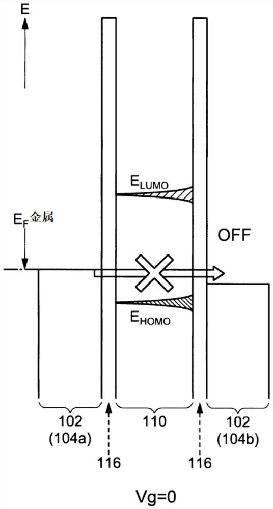
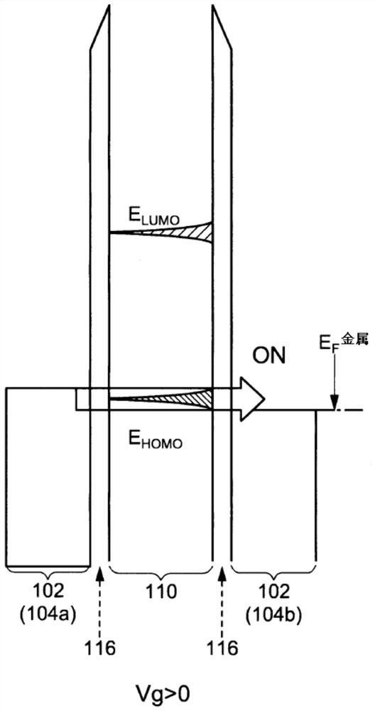
[0164] The following is a fabrication example of a single molecular transistor. The monomolecular transistor fabricated in this example has the same Figure 6A , Figure 6B , Figure 6C The same configuration as the single-molecule transistor described in .

[0165] 4-1 Fabrication of Nanogap Electrodes

[0166] The steps of preparing the nanogap electrodes include the steps of making platinum electrodes as the first electrode layer 106a and the second electrode layer 106b, and growing gold particles on the platinum electrodes as the first metal particles 108a and the second metal particles by electroless gold plating. Step 108b.

[0167] 4-1-1 Manufacture of Platinum Electrode

[0168] As a substrate for producing a platinum electrode, a silicon wafer having a silicon oxide film formed on its surface was used. The substrate is cleaned by ultrasonic cleaning using acetone and ethanol, ultraviolet (UV) ozone...

Embodiment 2

[0229] This example shows the characteristics of a single-molecule transistor using a different functional molecule from Example 1. In this embodiment, the structure of the unimolecular transistor is the same as that of the first embodiment. The fabrication of the nanogap electrodes was carried out according to the same procedure as that of the first embodiment. As a functional molecule, a carbon-bridged p-phenylene vinylene oligomer (COPV6(SH) 2 ). The steps of introducing functional molecules into the nanogap electrodes are the same as those in the first embodiment.

[0230] 6-1 carbon bridge p-phenylene vinylene oligomer (COPV6(SH) 2 )Structure

[0231] Carbon-bridged p-phenylene vinylene oligomer (COPV6(SH) 2 ) structure is represented by formula (6).

[0232] [chemical formula 6]

[0233]

[0234] R 1 to R 3 Can be the same or different. R 1 to R 3 May be the same or different aryl substituents which may be substituted. The aryl group is preferably a hydro...

Embodiment 3

[0258] This example shows a single-molecule transistor using both ends of a silicon-bridged quinone-type condensed oligomeric silanol derivative (Si-2×2) as a rigid π-conjugated molecule containing silicon. Contains -O-(CH 2 ) n Single molecules of SH serve as functional molecules.

[0259] 7-1 Fabrication method of single molecular transistor

[0260] A nanogap electrode was fabricated in the same manner as in Example 1. The fabricated nanogap electrodes were impregnated in hexanethiol (C 6 SH) solution, a self-assembled monolayer (SAM: Self-Assembled Monolayer) was prepared. When the surface coverage of the SAM is intentionally reduced by shortening the immersion time, the introduction rate of functional molecules having linking groups and anchoring groups is increased.

[0261] In addition, the SAM is effective for fabricating a bridge-structured unimolecular transistor in which a functional molecule having a linking group and an anchoring group at both ends is chemicall...


PUM

PropertyMeasurementUnit
Lengthaaaaaaaaaa
Conductanceaaaaaaaaaa
Gap lengthaaaaaaaaaa

Abstract

A unimolecular transistor according to the present invention includes: a first electrode having a first electrode layer and a first metal particle disposed at one end section of the first electrode layer; a second electrode having a second electrode layer and a second metal particle disposed at one end section of the second electrode layer; a third electrode insulated from the first electrode andthe second electrode; and a pai-conjugated molecule having a pai-conjugated skeleton. The first electrode and the second electrode are disposed such that the first metal particle and the second metalparticle face each other with a gap therebetween. The width from one end to the other end of each of the first metal particle and the second metal particle is 10 nm or less. The third electrode is disposed so as to be adjacent to the gap faced by the first metal particle and the second metal particle and so as to be separated from the first metal particle and the second metal particle. The pai-conjugated molecule is disposed in the gap between the first metal particle and the second metal particle.

Description

technical field [0001] The present invention relates to a molecular device, and relates to a transistor in which a region corresponding to a channel is composed of molecules, and electrons or holes flow through quantum effects. Background technique [0002] Semiconductor integrated circuits have achieved remarkable development along with the advancement of miniaturization technology. However, with miniaturization, several problems also appeared. For example, various problems have been pointed out: increase of off-leakage current due to short channel effect of transistors, increase of gate leakage current due to thinning of the gate insulating film, CMOS (Complementary Metal Oxide Semiconductor) structure The upper limit of the operating speed, the increase in power consumption, and the increase in parasitic capacitance due to high-density wiring. [0003] Facing the limitations of such technological progress, research for realizing new electronic devices is being conducted...

Claims


Application Information

Patent Timeline
IPC IPC(8): H01L51/30H01L51/05H01L21/28H01L21/288H01L29/06H01L29/417H01L29/66H01L29/786
CPCH01L29/786H01L29/66H01L29/417H01L21/28H01L21/288H01L29/06H10K10/701H10K10/82H10K85/6574H10K10/481H10K10/484H10K10/84H10K30/671H10K85/114
Inventor 真岛豊中村栄一辻勇人野崎京子新谷亮欧阳春居藤悠马李昇柱
Owner JAPAN SCI & TECH CORP
Why Eureka
Try Eureka