Three-dimensional memory and forming method of three-dimensional memory

A memory, three-dimensional technology, applied in electric solid state devices, semiconductor devices, semiconductor/solid state device components, etc., can solve problems such as memory cell programming interference, and achieve better heat insulation effect

Inactive Publication Date: 2021-03-02
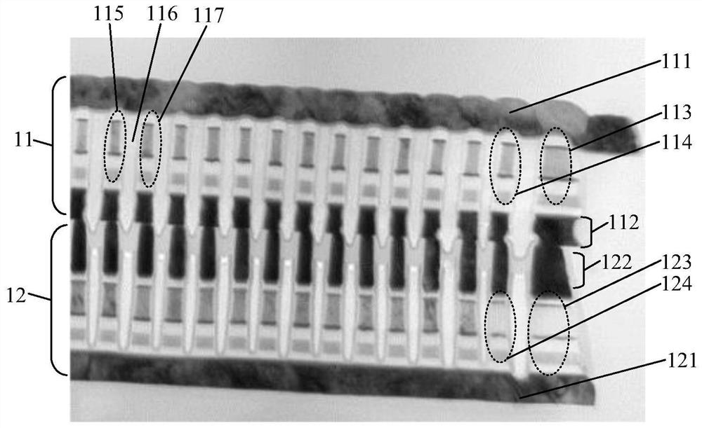
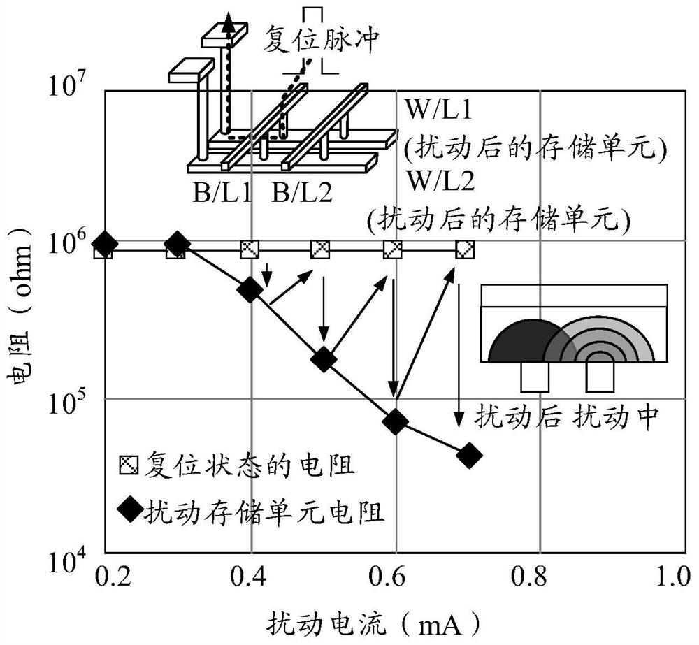
YANGTZE ADVANCED MEMORY INDUSTRIAL INNOVATION CENTER CO LTD
View PDF3 Cites 1 Cited by
  • Summary
  • Abstract
  • Description
  • Claims
  • Application Information

AI Technical Summary

Problems solved by technology

[0003] In related technologies, the distance between adjacent 3D XPoint memory cells is small, which means tha

Method used


Image

  • Three-dimensional memory and forming method of three-dimensional memory
  • Three-dimensional memory and forming method of three-dimensional memory
  • Three-dimensional memory and forming method of three-dimensional memory

Examples


Example Embodiment

[0089] Embodiment one

[0090] figure 2 A schematic diagram of an optional structure of the three-dimensional memory provided by the embodiment of the present application, such as figure 2 As shown, the three-dimensional memory 20 includes:

[0091] A plurality of first conductive lines 201 extend along a first direction.

[0092] Here, the first direction is the X-axis direction, and the material of the first conductive line 201 includes but not limited to tungsten (W), cobalt (Co), copper (Cu), aluminum (Al), polysilicon, doped silicon , silicide, or any combination thereof.

[0093] A plurality of second conductive lines 202 extend along a second direction, and the first direction and the second direction are perpendicular to each other.

[0094] In the embodiment of the present application, the second direction is the Y-axis direction, and the material of the second conductive line 202 includes but not limited to tungsten (W), cobalt (Co), copper (Cu), aluminum (Al),...

Example Embodiment

[0098] Embodiment two

[0099] Figure 3A An optional structural schematic diagram of the three-dimensional memory provided by the embodiment of the present application, such as Figure 3A As shown, the three-dimensional memory 30 includes:

[0100] A plurality of first conductive lines 301 extend along a first direction.

[0101] A plurality of second conductive lines 302 extend along a second direction, and the first direction and the second direction are perpendicular to each other.

[0102] In the embodiment of the present application, the first direction is the X-axis direction, the second direction is the Y-axis direction, and the materials of the first conductive wire 301 and the second conductive wire 302 include but are not limited to tungsten (W ), cobalt (Co), copper (Cu), aluminum (Al), polysilicon, doped silicon, silicide, or any combination thereof.

[0103] In some embodiments, the three-dimensional memory 30 further includes: arranged between the first cond...

Example Embodiment

[0123] Embodiment Three

[0124] Figure 4A A schematic diagram of the implementation flow of the method for forming a three-dimensional memory provided in the embodiment of the present application, as shown in Figure 4A As shown, the method includes the following steps:

[0125] Step S401, forming a semiconductor stack structure.

[0126] The semiconductor stack structure 41 is a stack structure with a certain number of layers. In the embodiment of the present application, the semiconductor stack structure 41 can be formed by chemical vapor deposition (Chemical Vapor Deposition, CVD) or physical vapor deposition (Physical Vapor Deposition, PVD) Or atomic layer deposition (Atomic Layer Deposition, ALD) and other methods are formed on the surface of the substrate (not shown in the figure). Figure 4B A schematic cross-sectional structure diagram of a semiconductor stack structure provided in an embodiment of the present application, Figure 4B A schematic cross-sectional v...


PUM

PropertyMeasurementUnit
Thermal conductivityaaaaaaaaaa
Thermal stabilityaaaaaaaaaa
Surface areaaaaaaaaaaa

Abstract

An embodiment of the invention discloses a three-dimensional memory and a forming method of the three-dimensional memory. The three-dimensional memory comprises a plurality of first conductive wires which extend along a first direction, a plurality of second conductive lines extending in a second direction, and a plurality of phase change memory units, wherein the first direction and the second direction are perpendicular to each other; the plurality of phase change memory units are arranged between the first conductive wire and the second conductive wire and are perpendicular to the first conductive wire and the second conductive wire; and a gap exists between two adjacent phase change storage units, the gap is filled with a heat insulation material, and a heat conductivity coefficient ofthe heat insulation material is lower than a threshold value.

Description

technical field [0001] The embodiment of the present application relates to the field of semiconductor technology, and relates to but not limited to a three-dimensional memory and a method for forming the three-dimensional memory. Background technique [0002] In commercial three-dimensional memory, such as three-dimensional phase change memory (Three Dimensional Phase ChangeMemory, 3D PCM), word line (Word Line, WL) and bit line (Bit Line, BL) are formed by patterning process after 20nm / 20nm etc. Line width (Line / Space, L / S) composition. The memory cells are placed at the intersection between the mutually perpendicular WL and BL, forming a cross-point architecture (3D Xpoint). [0003] In the related art, the distance between adjacent 3D XPoint memory cells is small, which means that there is potential thermal crosstalk, which will cause programming interference between adjacent memory cells. When the size of the three-dimensional memory is made smaller, the thermal cross...

Claims


Application Information

Patent Timeline
IPC IPC(8): H01L27/24H01L23/367H01L23/373
CPCH01L23/367H01L23/373H01L23/3737H10B63/84
Inventor 刘峻
Owner YANGTZE ADVANCED MEMORY INDUSTRIAL INNOVATION CENTER CO LTD
Why Eureka
Try Eureka