
Decoupling capacitor placement method applied to system-in-package

A technology of system-level packaging and decoupling capacitors, which is applied in the direction of circuits, electrical components, and electrical solid-state devices, and can solve problems such as occupying space

Inactive Publication Date: 2021-03-05
TIANJIN UNIV MARINE TECH RES INST
View PDF5 Cites 0 Cited by
  • Summary
  • Abstract
  • Description
  • Claims
  • Application Information

AI Technical Summary

Problems solved by technology

However, since interconnection using gold wires takes up space, the system-in-package can still be optimized to provide space for decoupling capacitors

Method used


Image

  • Decoupling capacitor placement method applied to system-in-package
  • Decoupling capacitor placement method applied to system-in-package
  • Decoupling capacitor placement method applied to system-in-package

Examples


Embodiment Construction

[0016] A decoupling capacitor placement method applied to system-in-package, specifically:

[0017] Step 1, according to the overall routing requirements, preset the substrates Sub1 and Sub2;

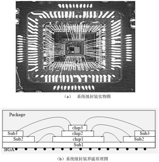
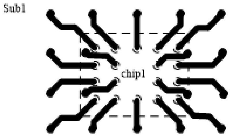
[0018] Step 2, flip the bottom chip1 over, discard the original gold wire interconnection, and use fan out interconnection, such as figure 2 , making full use of the space of the bottom substrate (Sub1); since the other two chips do not have fan-out interconnection conditions, the gold wire interconnection method is still used;

[0019] Step 3, adjust the original interconnection position of the gold wires so that chip2 is connected to Sub1, and chip3 is connected to Sub2; this adjustment can firstly vacate the space of Sub3, and the gold wire routing is steeper, reducing the waste of space;

[0020] Step 4, replace the original position of Sub3 with a ring capacitor, such as image 3 , according to the normal size of the chip, this capacitor will be sufficient for the decoupling nee...


PUM


Abstract

The invention discloses a decoupling capacitor placement method applied to the system-in-package. Firstly, the interconnection mode is optimized, the space efficiency of the 3D system-in-package is further saved, and due to the fact that gold wire interconnection is reduced, the signal transmission quality is slightly improved. Then, the decoupling capacitor is placed in the residual space in thepackage, so that the problem that the space occupied by the decoupling capacitor is too large is solved, and the signal integrity is further improved. By optimizing the interconnection mode between different layers of system-in-package and the chip, a placement space is provided for the decoupling capacitor, and finally the power supply and signal integrity performance of the system is optimized.

Description

technical field [0001] The invention relates to the field of integrated circuits, in particular to a design for suppressing power supply noise by using decoupling capacitors, that is, a method for placing decoupling capacitors applied to system-level packaging. Background technique [0002] Power supply noise has always been the focus of signal quality research. Power supply noise can cause problems such as signal high and low level blurring, signal jitter and so on. There are various parasitic parameters such as parasitic inductance, parasitic resistance, parasitic capacitance, and conductance in the power ground plane pair, which are very different from the ideal power ground plane pair in conventional simulations. The centering of the power ground plane often causes voltage fluctuations due to the charging and discharging current of the components. Designers often use decoupling capacitors to address this type of power supply noise. Both on-chip capacitors and off-chip...

Claims


Application Information

Patent Timeline
IPC IPC(8): H01L21/98H01L25/16
CPCH01L25/50H01L25/16
Inventor 徐江涛于东哲聂凯明高静高志远
Owner TIANJIN UNIV MARINE TECH RES INST
Learn More