SOI MOS structure capable of resisting edge electric leakage and forming method thereof

A technology of edge leakage and leakage area, which is applied in the direction of circuits, electrical components, semiconductor devices, etc., can solve the problems of parasitic transistor turn-on and affect the electrical characteristics of MOS devices, etc., and achieve the effect of suppressing turn-on

Pending Publication Date: 2021-03-09
INST OF MICROELECTRONICS CHINESE ACAD OF SCI
View PDF0 Cites 2 Cited by
  • Summary
  • Abstract
  • Description
  • Claims
  • Application Information

AI Technical Summary

Problems solved by technology

Although LOCOS and STI technologies have good isolation effects, they also introduce parasitic transistor effects. If the process is not handled properly or in an ionizing radiation environment, the parasitic transistors will be turned on, which will seriously affect the electrical characteristics of MOS devices.

Method used


Image

  • SOI MOS structure capable of resisting edge electric leakage and forming method thereof
  • SOI MOS structure capable of resisting edge electric leakage and forming method thereof
  • SOI MOS structure capable of resisting edge electric leakage and forming method thereof

Examples


Embodiment Construction

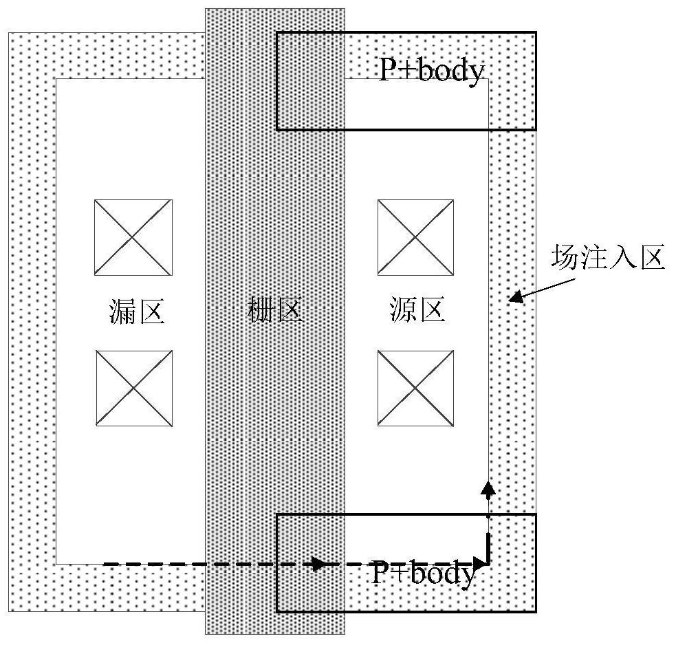
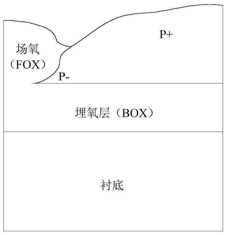
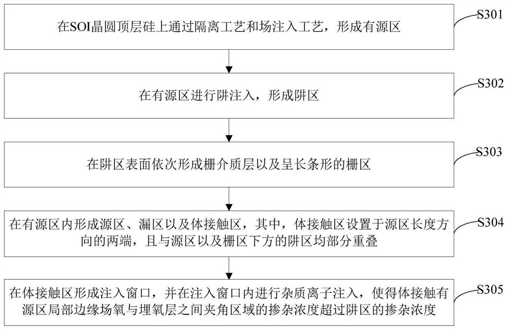
[0031] Exemplary embodiments of the present disclosure will be described in more detail below with reference to the accompanying drawings. Although exemplary embodiments of the present disclosure are shown in the drawings, it should be understood that the present disclosure may be embodied in various forms and should not be limited by the embodiments set forth herein. Rather, these embodiments are provided for more thorough understanding of the present disclosure and to fully convey the scope of the present disclosure to those skilled in the art.

[0032] Various structural schematic diagrams according to embodiments of the present disclosure are shown in the accompanying drawings. The figures are not drawn to scale, with certain details exaggerated and possibly omitted for clarity of presentation. The shapes of the various regions and layers shown in the figure, as well as their relative sizes and positional relationships are only exemplary, and may deviate due to manufactur...


PUM

PropertyMeasurementUnit
Doping concentrationaaaaaaaaaa

Abstract

The invention discloses an SOI MOS structure capable of resisting edge electric leakage and a forming method thereof. The structure is characterized in that a heavily-doped region is arranged in a body contact region, the doping concentration of the heavily-doped region exceeds the doping concentration of a well region, the heavily-doped region comprises a partial boundary region between a body contact active region and a field injection region, and the edge of the heavily doped region is spaced apart from the gate region by a preset distance, so that the doping concentration of an included angle region between the body contact active region local edge field oxygen and the buried oxide layer exceeds the doping concentration of the well region, the injection window exposes the partial boundary region between the body contact active region and the field injection region, and a certain spacing distance is formed between the edge of the injection window and the gate region. Through the method, the parasitic transistor effect can be effectively inhibited, and a BTS-type SOI MOS structure capable of resisting edge electric leakage is formed.

Description

technical field [0001] The invention relates to the technical field of semiconductors, in particular to an anti-edge leakage SOI MOS structure and a forming method thereof. Background technique [0002] SOI (Silicon On Insulator, silicon on insulator) is a silicon material with a special structure. SOI technology includes very rich content, such as materials, devices and integrated circuit manufacturing technologies. For SOI CMOS technology, due to the use of full dielectric isolation between devices, compared with bulk silicon technology, it has the advantages of no parasitic latch, high speed, low power consumption, high temperature resistance and radiation resistance. [0003] However, the leakage current of SOI MOSFET devices has always been an urgent problem to be solved in the industry. Currently commonly used isolation process technologies include junction isolation, LOCOS (Local Oxidation of Silicon, local oxidation isolation of silicon) technology, and STI (Shallow...

Claims


Application Information

Patent Timeline
IPC IPC(8): H01L29/78H01L29/06H01L29/36H01L21/336
CPCH01L29/78H01L29/0607H01L29/0684H01L29/36H01L29/66477
Inventor 曾传滨高林春李晓静闫薇薇单梁李多力倪涛王娟娟罗家俊韩郑生
Owner INST OF MICROELECTRONICS CHINESE ACAD OF SCI
Why Eureka
Try Eureka