Supercharge Your Innovation With Domain-Expert AI Agents!

Optical signal driven two-dimensional logic switch and preparation method thereof

A logic switch, optical signal technology, applied in the direction of logic circuits using optoelectronic devices, logic circuits using specific components, and final product manufacturing, etc., can solve problems such as inability to detect and increase the complexity of devices

Active Publication Date: 2021-03-23
UNIV OF SCI & TECH BEIJING
View PDF4 Cites 0 Cited by
  • Summary
  • Abstract
  • Description
  • Claims
  • Application Information

AI Technical Summary

Problems solved by technology

The output current of the phototransistor is usually very small, at the level of microamperes, and cannot be effectively detected by the logic circuit as an input signal. Usually, a current amplifier is selected to amplify the signal, but it will increase the complexity of the device. There is no need to use an amplifier to directly convert the phototransistor The generated output signal is passed to the logic circuit, there are many problems and challenges

Method used


Image

  • Optical signal driven two-dimensional logic switch and preparation method thereof

Examples


Embodiment Construction

[0038] In order to make the object, technical solution and advantages of the present invention clearer, the implementation manner of the present invention will be further described in detail below in conjunction with the accompanying drawings.

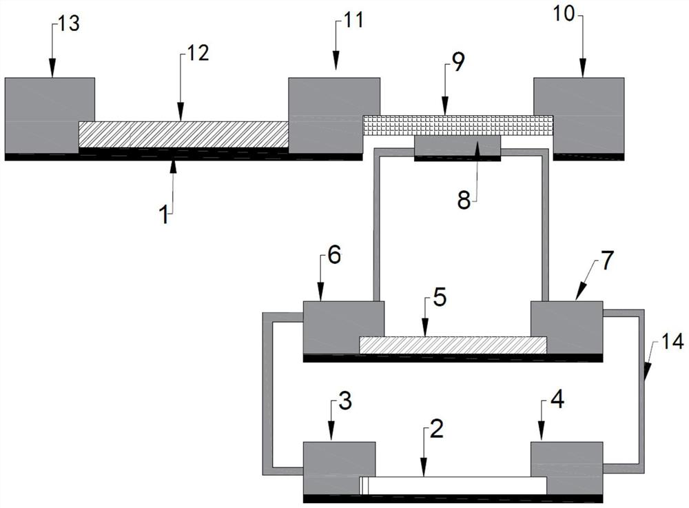
[0039] Such as figure 1 As shown, this embodiment provides a two-dimensional logic switch driven by an optical signal. The two-dimensional logic switch includes a substrate 1 and a two-dimensional molybdenum ditelluride 2 integrated on the substrate 1, a first electrode 3, a second Two electrodes 4 , amplifying resistor 5 , third electrode 6 , fourth electrode 7 , fifth electrode 8 , two-dimensional molybdenum disulfide 9 , sixth electrode 10 , seventh electrode 11 , logic resistor 12 and eighth electrode 13 .

[0040] The substrate 1, the two-dimensional molybdenum ditelluride 2, the first electrode 3 and the second electrode 4 form a phototransistor, and the phototransistor is a field effect transistor; wherein, the substrate 1 is us...


PUM

PropertyMeasurementUnit
Thicknessaaaaaaaaaa
Lengthaaaaaaaaaa
Thicknessaaaaaaaaaa

Abstract

The invention discloses an optical signal driven two-dimensional logic switch and a preparation method thereof. The switch comprises a phototransistor, an amplification resistor, a logic transistor and a logic resistor; the phototransistor is composed of a substrate, two-dimensional molybdenum ditelluride and an electrode; the amplification resistor is composed of an electrode and two-dimensionalboron nitride; the logic transistor is composed of a substrate, two-dimensional molybdenum disulfide and an electrode; the logic resistor is composed of an electrode and two-dimensional boron nitride;the two ends of the amplification resistor are connected to the source electrode and the drain electrode of the phototransistor in parallel, and current signals output by the phototransistor are converted into voltage signals, and the amplification resistor plays an amplifying role; the logic transistor is connected with the logic resistor in series; the electric signals generated by the phototransistor are transmitted to the grid electrode of the logic transistor in a grid voltage mode through the amplification resistor, finally the electric signals are output from the drain electrode of thelogic transistor; and therefore, optical signal driven logic output is achieved. According to the optical signal driven two-dimensional logic switch, a current amplifier is not needed, so that the preparation process is simplified, and the size of the device is reduced.

Description

technical field [0001] The invention relates to the technical field of semiconductor optoelectronic integration, in particular to a two-dimensional logic switch driven by an optical signal and a preparation method thereof. Background technique [0002] Since the 21st century, the world has fully entered the electronic information age. In order to meet the huge needs of the electronics industry, the semiconductor integrated circuit industry has made great progress. Two-dimensional materials and related devices have sprung up suddenly, and have a wide range of applications in a new generation of optoelectronic devices, such as photodetectors, logic devices, and memories. Therefore, the preparation of two-dimensional materials and related device construction technology has always been an international research hotspot and one of the main technical fields of competition in various countries. Due to their ultrahigh carrier mobility, easy integration and broadband light absorpti...

Claims


Application Information

Patent Timeline
IPC IPC(8): H01L27/144H01L31/18H03K19/14
CPCH01L27/1443H01L31/18H03K19/14Y02P70/50
Inventor 张跃黄梦婷张铮汤文辉杜君莉刘璇王利华
Owner UNIV OF SCI & TECH BEIJING
Features
  • R&D
  • Intellectual Property
  • Life Sciences
  • Materials
  • Tech Scout
  • Unparalleled Data Quality
  • Higher Quality Content
  • 60% Fewer Hallucinations
Learn More