Array substrate, preparation method thereof and display panel

An array substrate and side surface technology, applied in the field of display devices, can solve the problems of excessive ITO engraving on the top layer, PDL overlap problem, short circuit between pixels, etc., to prevent ITO residue problems, improve yield, and improve the effect of reflectivity

Active Publication Date: 2021-03-23
WUHAN CHINA STAR OPTOELECTRONICS SEMICON DISPLAY TECH CO LTD
View PDF5 Cites 2 Cited by
  • Summary
  • Abstract
  • Description
  • Claims
  • Application Information

AI Technical Summary

Problems solved by technology

Among them, a large area of ​​anode residue may cause a short circuit problem between pixels, and too much ITO on the top layer is over-etched, resulting in the problem of exposing silver.
like figure 1 and figure 2 As shown, when the etching process of the anode is wet-etched, the "undercut" phenomenon generally occurs, resulting in abnormal slope angles, which in turn leads to PDL (pixel definition layer) overlapping problems

Method used


Image

  • Array substrate, preparation method thereof and display panel
  • Array substrate, preparation method thereof and display panel
  • Array substrate, preparation method thereof and display panel

Examples


Embodiment Construction

[0026] The technical solutions in the embodiments of the present application will be clearly and completely described below in conjunction with the drawings in the embodiments of the present application. Apparently, the described embodiments are only some of the embodiments of this application, not all of them. Based on the embodiments in this application, all other embodiments obtained by those skilled in the art without making creative efforts belong to the scope of protection of this application.

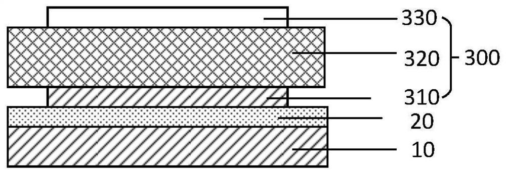
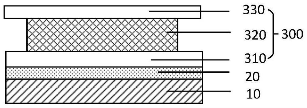
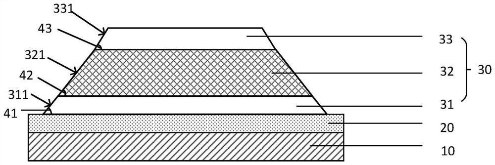
[0027] See image 3 , image 3 It is a schematic structural diagram of a compound electrode of an array substrate in the present application; in this embodiment, an array substrate is provided. Such as image 3 As shown, the array substrate includes a thin film transistor layer 10, a planar layer 20, and a composite electrode layer 30 stacked in sequence, wherein the thin film transistor layer 10 includes an array arranged on a base substrate (not shown in the figure). ) at l...


PUM

PropertyMeasurementUnit
transmittivityaaaaaaaaaa

Abstract

The invention discloses an array substrate, which comprises a flat layer and a composite electrode arranged on the flat layer, wherein at least one undercut structure is formed by the side surface ofthe edge of the composite electrode and the surface of the flat layer, the composite electrode comprises at least one metal electrode and at least one transparent electrode, and the metal electrodes and the transparent electrodes are alternately stacked.

Description

technical field [0001] The present application relates to the technical field of display devices, in particular to an array substrate, a manufacturing method thereof, and a display panel. Background technique [0002] Flexible AMOLED screens have injected new vitality into the display industry, but the yield rate has always been an important issue it faces, and improving the yield rate is the primary task that panel manufacturers urgently need to solve. In the current AMOLED products, the film-forming temperature of ITO is room temperature (about 25°C), forming amorphous (a-ITO), and there will often be anode Pin Holes (plugged holes, bubbles) and anode "black spots" (sulfurization) , Abnormal pixel display, anode etching and other yield problems, please refer to figure 1 with figure 2 , figure 1 with figure 2 It is a structural schematic diagram of a composite electrode formed by wet etching in the prior art. The composite electrode 300 includes a first electrode 310...

Claims


Application Information

Patent Timeline
Patent Type & Authority Applications(China)
IPC IPC(8): H01L27/32H01L51/52H01L51/56G09F9/30
CPCG09F9/301H10K59/122H10K59/12H10K50/822H10K71/00
Inventor 张蕊
Owner WUHAN CHINA STAR OPTOELECTRONICS SEMICON DISPLAY TECH CO LTD
Why Eureka
Try Eureka