Large-chamfer-angle heterogeneous substrate-gallium nitride composite structure and growth method thereof
A technology of heterogeneous substrate and composite structure, applied in electrical components, semiconductor/solid-state device manufacturing, circuits, etc., can solve the problems that gallium nitride materials cannot form a flat surface, narrow steps, etc., to overcome difficulties in flatness and quality The effect of good, easy growing conditions
- Summary
- Abstract
- Description
- Claims
- Application Information
AI Technical Summary
Problems solved by technology
Method used
Image

Examples
Embodiment 1
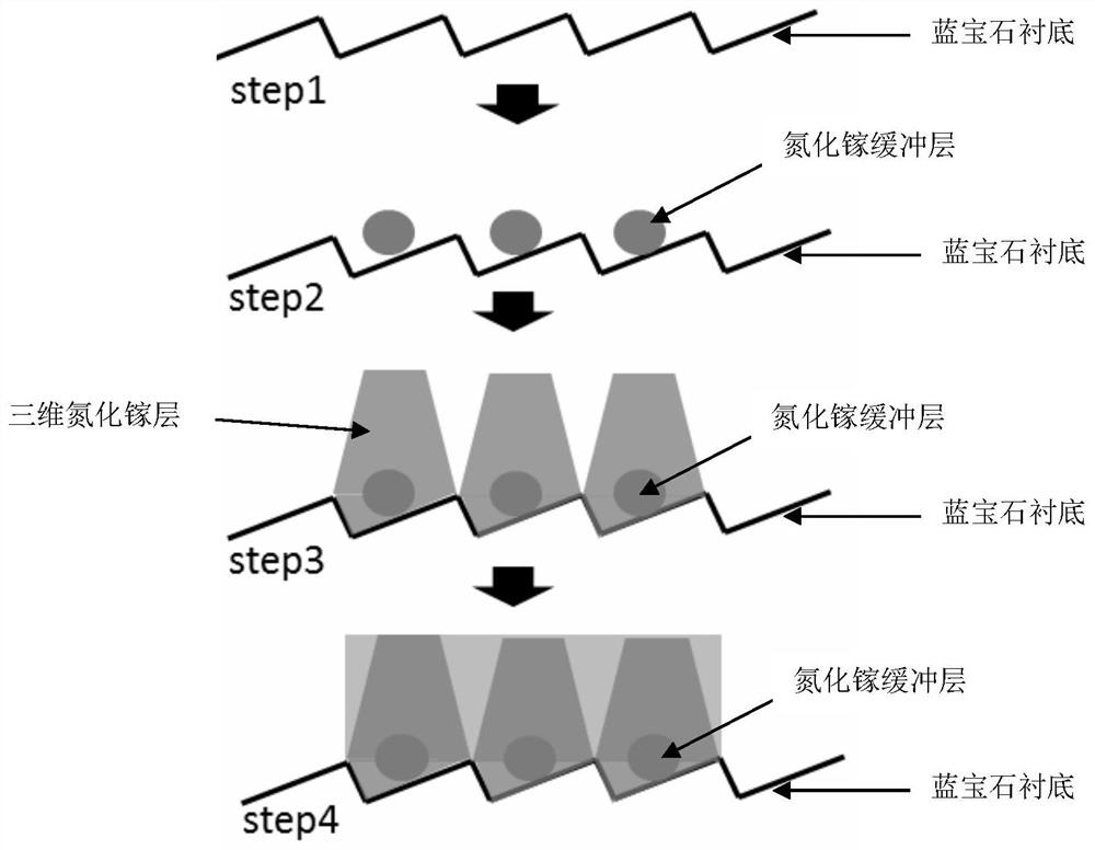
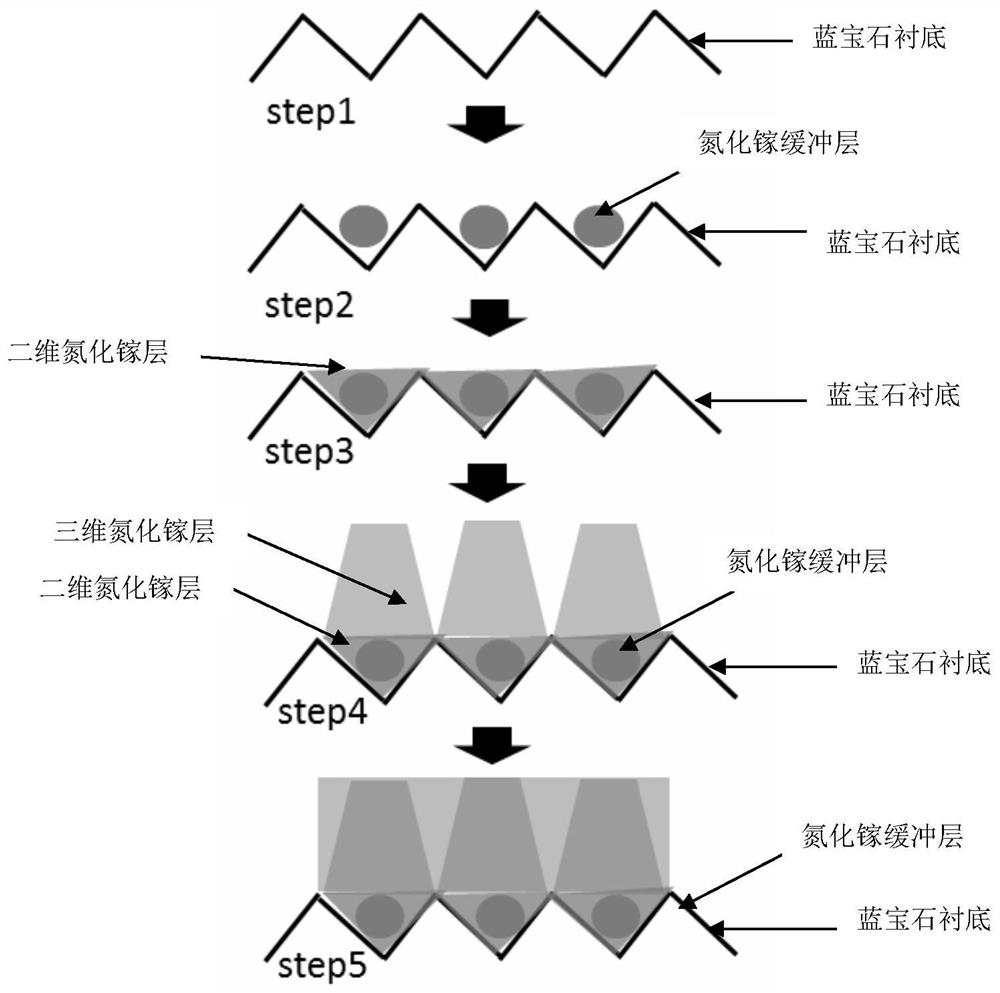
[0056] A heterogeneous epitaxial growth method based on "buffer layer-two-dimensional-three-dimensional underlying structure" includes:
[0057] 1) Place a large bevel angle sapphire substrate with a bevel angle of 1° in an epitaxial growth chamber, adjust the growth temperature in the growth chamber to 500°C, and the growth pressure to 600torr, and place the sapphire substrate with a large bevel angle A 25nm low-temperature GaN buffer layer is deposited on the bottom;
[0058] 2) Raise the growth temperature in the growth chamber to 1020°C, keep the growth pressure at 400torr, and perform annealing treatment on the low-temperature GaN buffer layer. The annealing time is 4 minutes. At this time, the low-temperature GaN buffer layer gathers at the steps to form islands ;
[0059] 3) Increase the growth temperature in the growth chamber to 1040°C, reduce the growth pressure to 50torr, and grow a 150nm two-dimensional GaN layer on the sapphire substrate with a large off-cut angl...
Embodiment 2
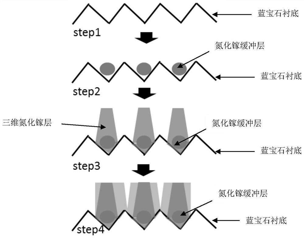
[0063] see image 3 , a heteroepitaxial growth method based on "buffer layer-two-dimensional-three-dimensional underlying structure" includes:
[0064] 1) Place a large bevel angle sapphire substrate with a bevel angle of 1° in an epitaxial growth chamber, adjust the growth temperature in the growth chamber to 530°C, and the growth pressure at 500torr, and place the sapphire substrate with a large bevel angle A 25nm low-temperature GaN buffer layer is deposited on the bottom;
[0065] 2) Raise the growth temperature in the growth chamber to 1040°C, and perform annealing treatment on the low-temperature GaN buffer layer, wherein the annealing time is 5 minutes, at this time, the low-temperature GaN buffer layer gathers at the steps to form an island shape;
[0066] 3) Increase the growth temperature in the growth chamber to 1060°C, reduce the growth pressure to 100torr, and grow a 150nm two-dimensional GaN layer on a sapphire substrate with a large off-cut angle at a growth ra...
Embodiment 3
[0070] see image 3 , a heteroepitaxial growth method based on "buffer layer-two-dimensional-three-dimensional underlying structure" includes:
[0071] 1) Place a large bevel angle sapphire substrate with a bevel angle of 1° in an epitaxial growth chamber, adjust the growth temperature in the growth chamber to 600°C, and the growth pressure to 400torr, and place the sapphire substrate with a large bevel angle A 25nm low-temperature GaN buffer layer is deposited on the bottom;
[0072] 2) Raise the growth temperature in the growth chamber to 1080°C, keep the growth pressure at 500torr, and anneal the low-temperature GaN buffer layer. The annealing time is 5 minutes. At this time, the low-temperature GaN buffer layer gathers at the steps to form islands shape;
[0073] 3) Increase the growth temperature in the growth chamber to 1080°C, reduce the growth pressure to 200torr, and grow a 150nm two-dimensional GaN layer on the sapphire substrate with a large off-cut angle at a gro...
PUM
| Property | Measurement | Unit |
|---|---|---|
| Growth temperature | aaaaa | aaaaa |
| Growth pressure | aaaaa | aaaaa |
| Growth temperature | aaaaa | aaaaa |
Abstract
Description
Claims
Application Information
 - R&D
- Intellectual Property
- Life Sciences
- Materials
- Tech Scout
- Unparalleled Data Quality
- Higher Quality Content
- 60% Fewer Hallucinations
Browse by: Latest US Patents, China's latest patents, Technical Efficacy Thesaurus, Application Domain, Technology Topic, Popular Technical Reports.
© 2025 PatSnap. All rights reserved.Legal|Privacy policy|Modern Slavery Act Transparency Statement|Sitemap|About US| Contact US: help@patsnap.com