Wafer scribing machine for chip processing

A dicing machine and wafer technology, applied in electrical components, semiconductor/solid-state device manufacturing, circuits, etc., can solve the problem of increasing the friction between the wafer and the dicing device, reducing the reliability of the wafer dicing machine, and increasing the dicing damage. probability and other issues, to achieve the effect of high practicability, reducing friction and improving reliability

Inactive Publication Date: 2021-03-26
夏志强
View PDF0 Cites 1 Cited by
  • Summary
  • Abstract
  • Description
  • Claims
  • Application Information

AI Technical Summary

Problems solved by technology

[0003] When the existing wafer dicing machine is dicing the wafer, the debris generated is easy to adhere to the wafer, which will increase the friction between the wafer and the dicing device, thereby reducing the accuracy of the division. Not only that, when the existing wafer dicing machine is working, because the dicing on the dicing device rotates at a high speed, the temperature of the dicing itself is relatively high. If it is not dissipated in time, the consumption of the dicing will be accelerated. The service life of the chip increases the probability of damage to the dicing chip and reduces the reliability of the existing wafer dicing machine

Method used


Image

  • Wafer scribing machine for chip processing
  • Wafer scribing machine for chip processing
  • Wafer scribing machine for chip processing

Examples


Embodiment Construction

[0031] The present invention is described in further detail now in conjunction with accompanying drawing. These drawings are all simplified schematic diagrams, which only illustrate the basic structure of the present invention in a schematic manner, so they only show the configurations related to the present invention.

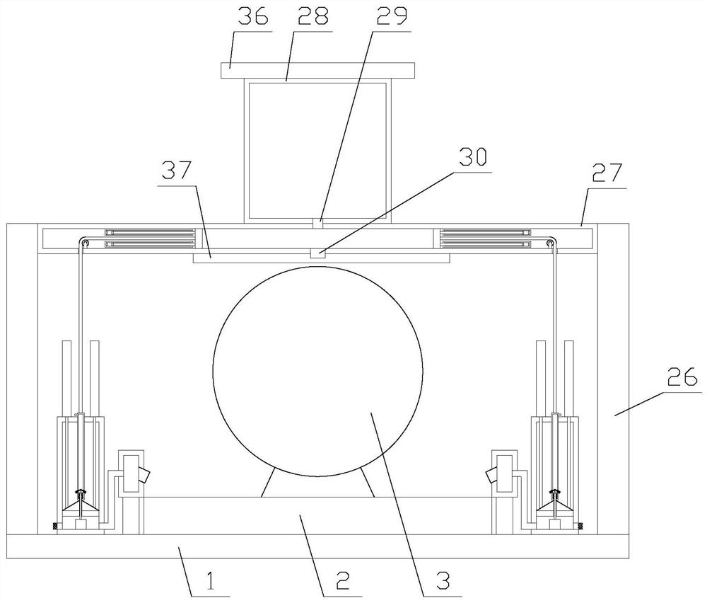
[0032] Such as figure 1 As shown, a wafer dicing machine for chip processing includes a base plate 1, a dicing device 3 and a workbench 2, and the dicing device 3 and the workbench 2 are fixed above the base plate 1, and the base plate 1 is equipped with a PLC, and also includes a cooling mechanism and two cleaning mechanisms. The two cleaning mechanisms are respectively arranged on both sides of the workbench 2. connect;

[0033] PLC, that is, programmable logic controller, is generally used for data processing and command receiving and output, and is used to realize central control. The user places the wafer on the workbench 2, and then controls the dicin...


PUM


Abstract

The invention relates to a wafer scribing machine for chip processing, which comprises a bottom plate, a scribing device, a workbench, a cooling mechanism and two cleaning mechanisms, wherein each cleaning mechanism comprises a fixed box, a fixed column, an air cylinder, a piston, an air inlet pipe, an air outlet pipe, a filter screen, an oiling assembly, a fixed block, a driving block, a connecting rope and two air cylinders; wherein the oiling assembly comprises an oiling box, a driving plate, a driving rod, a power rod, two first springs and two oiling units, the cooling mechanism comprisesa water tank, a water inlet pipe, a water spraying pipe, a supporting box, two water squeezing assemblies and two supporting rods, and each water squeezing assembly comprises a moving plate and two limiting units. According to the wafer scribing machine, through the cleaning mechanisms, the impurity removing function is achieved, the friction force between the scribing device and the wafer is prevented from being increased due to adhesion of chippings, so that the scribing work is prevented from being influenced, the scribing quality is improved, the function of cooling the scribing device isachieved through the cooling mechanism, and the scribing device is prevented from being damaged due to overheating.

Description

technical field [0001] The invention relates to the field of chips, in particular to a wafer dicing machine for chip processing. Background technique [0002] Wafer dicing is an essential process in the semiconductor chip manufacturing process. The whole wafer of the finished chip is divided into single chips according to the chip size, which is called wafer dicing. [0003] When the existing wafer dicing machine is dicing the wafer, the debris generated is easy to adhere to the wafer, which will increase the friction between the wafer and the dicing device, thereby reducing the accuracy of the division. Not only that, when the existing wafer dicing machine is working, because the dicing on the dicing device rotates at a high speed, the temperature of the dicing itself is relatively high. If it is not dissipated in time, the consumption of the dicing will be accelerated. The service life of the chip increases, thereby increasing the damage probability of the dicing chip and...

Claims


Application Information

Patent Timeline
Patent Type & Authority Applications(China)
IPC IPC(8): H01L21/78H01L21/82H01L21/822
CPCH01L21/78H01L21/82H01L21/822
Inventor 夏志强
Owner 夏志强
Why Eureka
Try Eureka