Intelligent insole, preparation method thereof and foot pressure monitoring system
A technology of smart insoles and hollow parts, applied in the field of flexible wear, can solve the problems of long-term high-precision sensing, elastic modulus, low flexibility, and affecting wearing comfort, and achieve low elastic modulus and capacitance Low relative rate of change and the effect of increasing the pressure range
- Summary
- Abstract
- Description
- Claims
- Application Information
AI Technical Summary
Problems solved by technology
Method used
Image
Examples
preparation example Construction
[0062] The preparation method of the smart insole of an embodiment, comprises the steps:
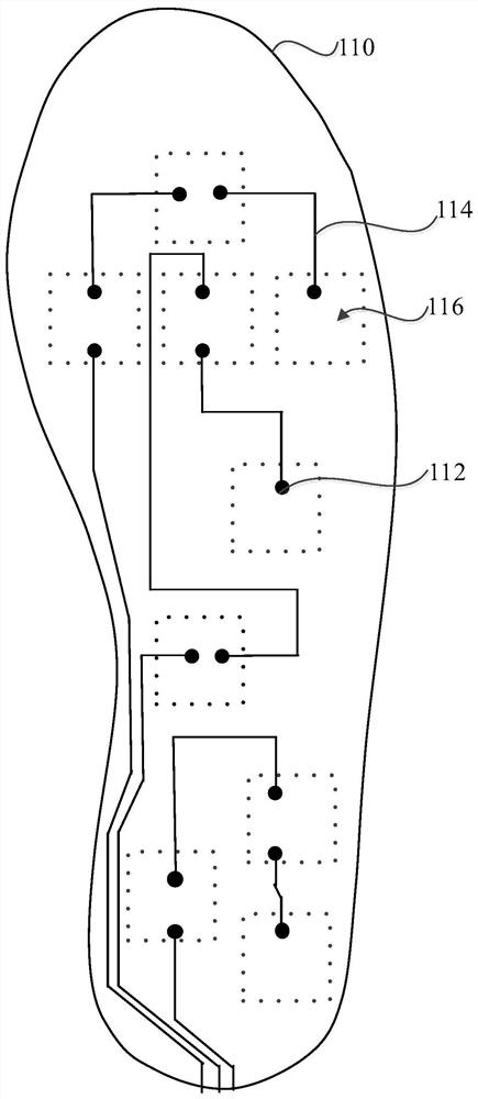
[0063] Step S110: making a first circuit board and a second circuit board, the first circuit board is provided with a plurality of first solder joints and wires for connecting the first solder joints, and the second circuit board is provided with a plurality of second solder joints point and a second wire for connecting to the second pad.
[0064] Wherein, both the first circuit board and the second circuit board are flexible circuit boards. For example, the material of the first circuit board and the second circuit board is PI or PET. Specifically, the thickness of the first circuit board is 0.1mm˜0.5mm. The thickness of the second circuit board is 0.1mm˜0.5mm.
[0065] In the first circuit board, the number and distribution of the first solder joints are related to the number and distribution of the array units in the sensor. The number of array units in the sensor determines the sp...
Embodiment 1
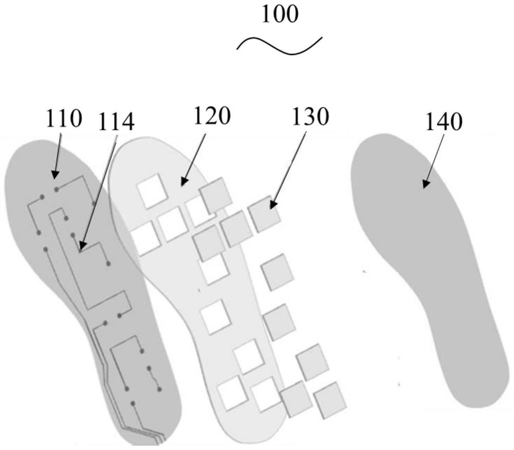
[0097] The structure of the smart insole of this embodiment is as image 3 As shown, it includes a first circuit board, a fill layer, a sensor and a second circuit board. Wherein, the sensor includes 9 array units, and each array unit includes a first electrode, a dielectric layer and a second electrode. The material of the filling layer is 3M VHB tape.
[0098] The preparation process of the smart insole of the present embodiment is as follows:
[0099] (1) The 3M VHB adhesive tape with 9 hollow parts corresponding to the first FPC circuit board is used as the filling layer, which is used for positioning the sensor on the first FPC circuit board, and is bonded to the first FPC circuit board, 9 The first hollow part hollows out the first solder joint on the first circuit board of the FPC.
[0100](2) A first electrode, a dielectric layer and a second electrode are sequentially formed at the hollow part to obtain a sensor composed of 9 array units. The specific steps are as...
Embodiment 2~ Embodiment 9
[0103] The structure and preparation process of the smart insoles of Examples 2 to 9 are similar to those of the smart insoles of Example 1, except that the material and thickness of the dielectric layer are different. The materials and thickness data of the dielectric layers in Examples 2 to 9 are shown in Table 1 below.
[0104] The material and the thickness of the dielectric layer of the embodiment of table 1
[0105] Example Mass ratio of PDMS precursor and curing agent Dielectric layer thickness / μm Example 2 20∶1 426 Example 3 20∶1 692 Example 4 20∶1 1270 Example 5 20∶1 1841 Example 6 10∶1 692 Example 7 15∶1 692 Example 8 20∶1 692 Example 9 30∶1 692
[0106] The following is the test part:
[0107] 1. Elastic modulus test
PUM
| Property | Measurement | Unit |
|---|---|---|
| thickness | aaaaa | aaaaa |
| thickness | aaaaa | aaaaa |
| thickness | aaaaa | aaaaa |
Abstract
Description
Claims
Application Information


