Method of implementing one or more void buried interposers in HPVE growth

A technology of inserting layers and voids, which is applied in the directions of single crystal growth, crystal growth, single crystal growth, etc., and can solve the problems of insignificant stress absorption effect and high cost

Inactive Publication Date: 2021-03-30
WUXI WUYUE SEMICON CO LTD
View PDF2 Cites 2 Cited by
  • Summary
  • Abstract
  • Description
  • Claims
  • Application Information

AI Technical Summary

Problems solved by technology

[0013] Aiming at the deficiencies of the prior art, the present invention provides a method for realizing one or more voids to bury the insertion layer in the growth of HPVE. One or more insertion layers can be used to obtain self-supporting materials with high quality, low

Method used


Image

  • Method of implementing one or more void buried interposers in HPVE growth
  • Method of implementing one or more void buried interposers in HPVE growth

Examples


Embodiment Construction

[0041] The technical solutions in the embodiments of the present invention will be clearly and completely described below in conjunction with the embodiments of the present invention. Obviously, the described embodiments are only some of the embodiments of the present invention, not all of them. Based on the embodiments of the present invention, all other embodiments obtained by persons of ordinary skill in the art without making creative efforts belong to the protection scope of the present invention.

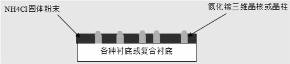
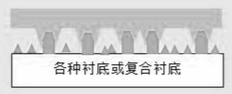
[0042] A method for realizing one or more void burying insertion layers in HPVE growth, is characterized in that, comprises the following steps:

[0043] (1) Use one of the following substrates or composite substrates:

[0044] (1), Al2O3, SCAM, Si, SiC substrate;

[0045] (II), Al2O3, SCAM, Si, SiC substrate with 10-100nm Sputtering AlN;

[0046] (III), Al2O3, SCAM, Si, SiC substrates with 0.2-10um MOCVD GaN film;

[0047] Place the substrate or composite substrate into th...


PUM


Abstract

The invention relates to the related technical field of gallium nitride production and preparation methods, and discloses a method for realizing one-time or multi-time hole burying of an insertion layer in HPVE growth, which comprises the following steps: (1) preparing one of the following substrates or composite substrates, comprising (I) Al2O3, SCAM, Si and SiC substrates, (II) preparing an Al2O3 substrate, an SCAM substrate, an Si substrate and an SiC substrate which are provided with Spring AlN, and (III) an Al2O3 substrate, an SCAM substrate, an Si substrate and an SiC substrate which areprovided with MOCVD GaN thin films; and placing the substrate or the composite substrate into an HVPE device for processing. The method for realizing the one-time or multi-time hole burying of the insertion layer in the HPVE growth comprises the following steps: firstly, forming a low-density and low-coverage gallium nitride crystal nucleus at a low temperature, and heating and annealing to forma high-quality small crystal; and then carrying out two-dimensional growth to form a gap layer in the interface and for absorbing stress during growth; in such a way, one or more layers are inserted to provide a template for the growth of self-supporting gallium nitride with high quality, low warpage and automatic interface stripping.

Description

technical field [0001] The invention relates to the related technical field of gallium nitride production and preparation methods, in particular to a method for realizing one or more holes to bury an insertion layer during HPVE growth. Background technique [0002] GaN is a typical representative of the third generation of wide bandgap semiconductors, has been widely used in semiconductor lighting, and has shown great application prospects in microwave power devices and power electronic devices. The most ideal substrate for gallium nitride growth is naturally gallium nitride single crystal material. Such homoepitaxial (that is, the epitaxial layer and the substrate are the same material) can greatly improve the crystal quality of the epitaxial film and reduce the dislocation density. , Improve the working life of the device, improve the luminous efficiency, and increase the working current density of the device. Conventional methods usually used for GaAs or Si, such as Czoc...

Claims


Application Information

Patent Timeline
IPC IPC(8): C30B29/40C30B25/18
CPCC30B29/406C30B25/186
Inventor 山本晓张海涛刘良宏许彬庞博
Owner WUXI WUYUE SEMICON CO LTD
Why Eureka
Try Eureka