Pulse interval-based noise elimination method and device for pulse image sensor

An image sensor and pulse interval technology, applied in the field of CMOS image sensor image processing, can solve the problems of contingency, the effect of noise removal is not obvious, and the noise in the time domain is not removed, and the noise in the time domain is eliminated, the noise removal effect is remarkable, and the space is eliminated. Effects of Domain Noise

Inactive Publication Date: 2021-03-30
THE ACAD OF TIANJIN UNIV HEFEI
View PDF5 Cites 3 Cited by
  • Summary
  • Abstract
  • Description
  • Claims
  • Application Information

AI Technical Summary

Problems solved by technology

[0005] The technical problem to be solved by the present invention lies in the fact that the existing technology has accidental and time-domain noise, and the noise removal effect is not obvious.

Method used


Image

  • Pulse interval-based noise elimination method and device for pulse image sensor
  • Pulse interval-based noise elimination method and device for pulse image sensor
  • Pulse interval-based noise elimination method and device for pulse image sensor

Examples


Embodiment 1

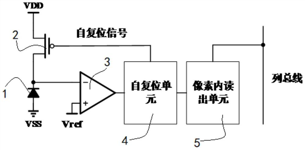
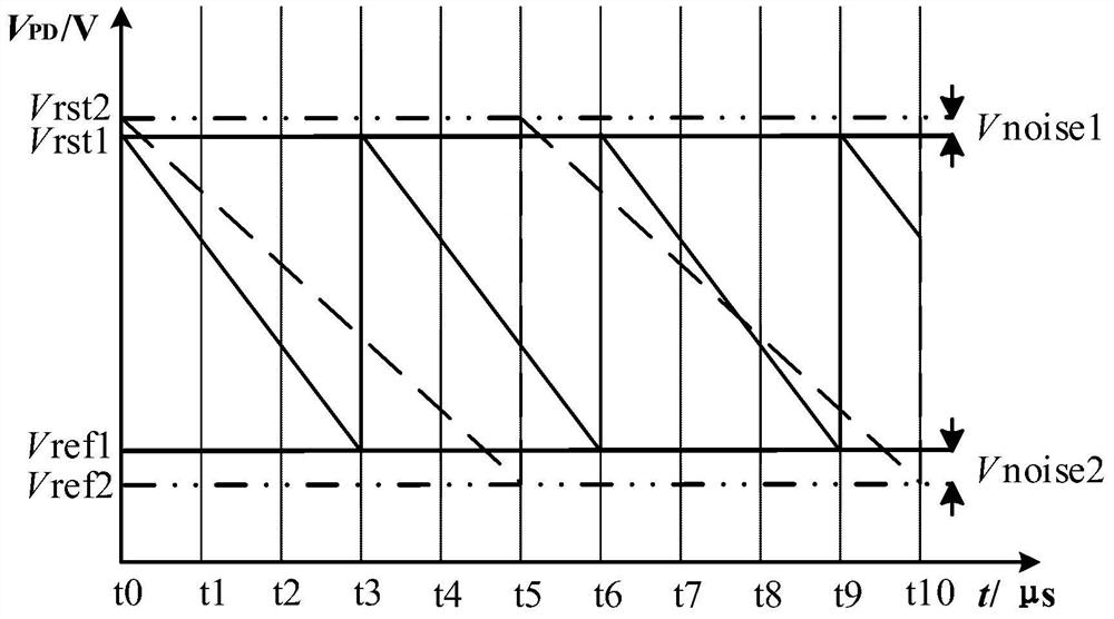
[0049] Noise elimination method for pulse image sensor based on pulse interval, applied to pulse pixel structure, such as figure 1 As shown, the pulse pixel structure includes a photodiode 1, a reset transistor 2, a comparator 3, a self-reset unit 4 and a readout unit 5 in the pixel, the anode of the photodiode 1 is connected to the power supply VSS, and the cathodes of the photodiode 1 are respectively connected to the reset The emitter of tube 2 and the inverting terminal of comparator 3, the collector of reset tube 2 is connected to the power supply VDD, and the non-inverting terminal of comparator 3 is connected to the threshold voltage V ref , the output terminal of the comparator 3 and the base of the reset transistor 2 are connected to the reset unit 4, the reset unit 4 is connected to the readout unit 5 in the pixel, and the readout unit 5 in the pixel is connected to the column bus. The working process of the pixel can be divided into three stages: In the integration ...

Embodiment 2

[0064] Corresponding to Embodiment 1 of the present invention, Embodiment 2 of the present invention also provides a pulse interval-based noise elimination device for a pulse image sensor, which is applied to a pulse pixel structure, and the device includes:

[0065] The first pulse interval acquisition module is used to obtain the first pulse interval of pixels caused by uniform illumination in consideration of time domain noise and space domain noise;

[0066] The second pulse interval acquisition module is used to consider the noise in the time domain and the noise in the space domain to obtain the second pulse interval of the pixel under no-light conditions;

[0067] A dark current coefficient matrix acquisition module, configured to acquire a dark current coefficient matrix according to the first pulse interval and the second pulse interval;

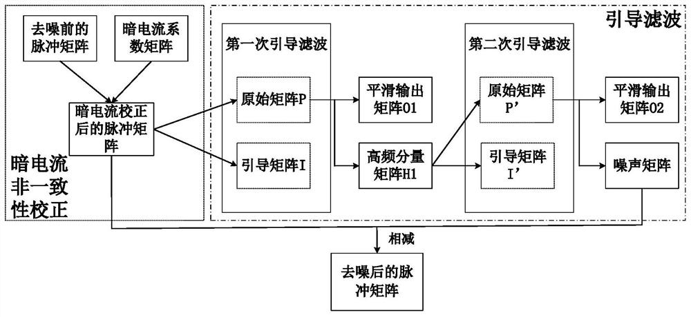
[0068] The denoising processing module is used to use the dark current coefficient matrix to perform dark current inconsistency co...


PUM


Abstract

The invention discloses a pulse interval-based pulse image sensor noise elimination method and device, applied to a pulse pixel structure; the method comprises the steps: obtaining a first pulse interval, caused by uniform illumination, of a pixel and a second pulse interval, under a dark condition, of the pixel in consideration of time domain noise and space domain noise; obtaining a dark currentcoefficient matrix; carrying out dark current non-consistency correction on the pulse matrix containing the noise by utilizing the dark current coefficient matrix to obtain a pulse matrix after darkcurrent correction, then carrying out guided filtering for multiple times to obtain a noise matrix, subtracting the noise matrix from the pulse matrix after dark current correction to obtain a denoised pulse matrix, and completing noise elimination. The method has the advantages that the pulse data is directly processed and the processing mode is simple and effective, so that the method has the potential of being implemented on hardware.

Description

technical field [0001] The invention relates to the field of image processing of CMOS image sensors, and more particularly relates to a method and device for eliminating noise of pulse image sensors based on pulse intervals. Background technique [0002] The pulse image sensor draws on the advantages of pulsed scene information in biological vision and complete information in frame rate image sensors, and converts all light intensity information into time-domain pulse signal representation, which has the characteristics of high speed, low data, and complete information. It solves the problems of the traditional frame rate image sensor that as the frame rate continues to increase, the amount of data will increase year-on-year, seriously affecting the data processing speed, and increasing the output pins, area and power consumption of the chip; while avoiding The address event indicates that the image sensor cannot effectively output the background information event due to the...

Claims


Application Information

Patent Timeline
Patent Type & Authority Applications(China)
IPC IPC(8): H04N5/361H04N5/365H04N5/359H04N5/374
CPCH04N25/625H04N25/671H04N25/63H04N25/76
Inventor 徐江涛徐亮高志远
Owner THE ACAD OF TIANJIN UNIV HEFEI
Why Eureka
Try Eureka