Optical transparent ultra-wideband radar and infrared double-stealth structure

An ultra-wideband radar, optically transparent technology, applied in the field of multi-spectrum stealth, can solve the problem of less attention to infrared stealth properties, achieve good optical transparency, improve infrared stealth performance, and reduce infrared emissivity.

Active Publication Date: 2021-04-09
AIR FORCE UNIV PLA
View PDF8 Cites 11 Cited by
  • Summary
  • Abstract
  • Description
  • Claims
  • Application Information

AI Technical Summary

Problems solved by technology

At present, researchers have designed and implemented a series of radar absorbers and scatterers with optical transparency properties, but their infrared stealth properties have received little attention

Method used


Image

  • Optical transparent ultra-wideband radar and infrared double-stealth structure
  • Optical transparent ultra-wideband radar and infrared double-stealth structure
  • Optical transparent ultra-wideband radar and infrared double-stealth structure

Examples


Embodiment 1

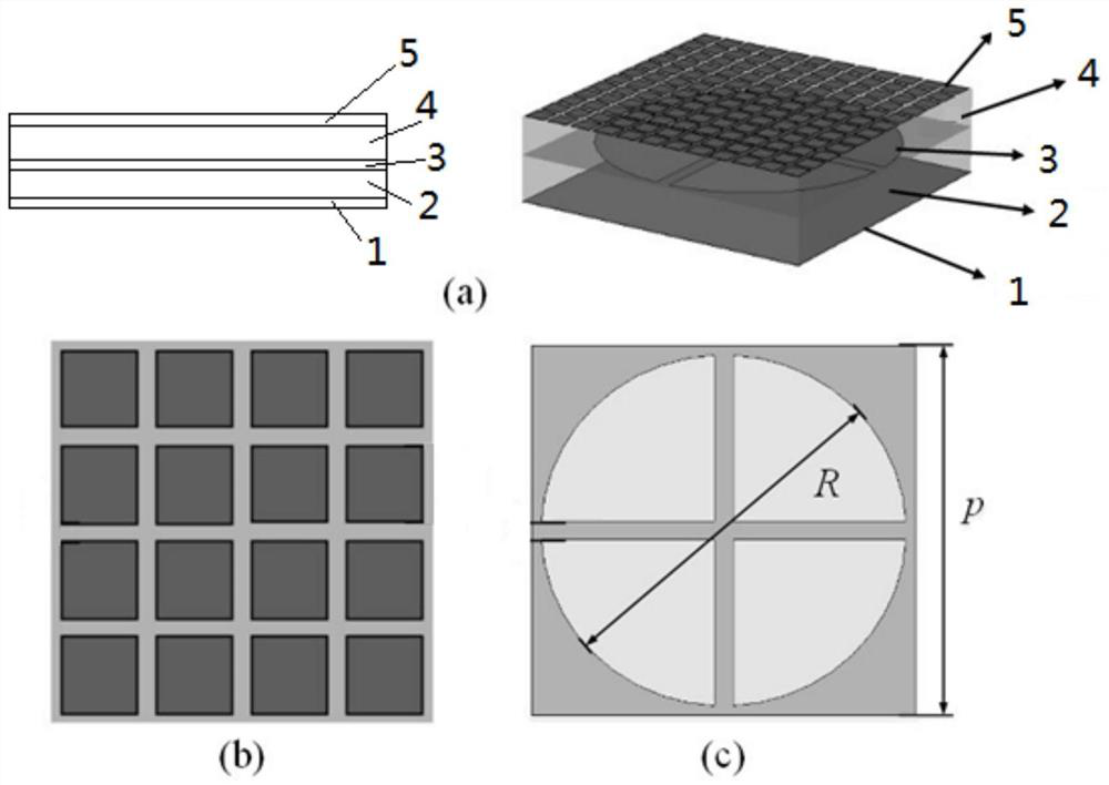
[0035] to combine figure 1 As shown, Embodiment 1 of the present invention provides an optically transparent ultra-wideband radar and infrared double stealth structure, including a low-emissivity infrared stealth layer and an ultra-wideband radar absorbing layer, which is a layered structure, including a backplane 1 from bottom to top , the first intermediate dielectric layer 2 , the first frequency selective surface layer 3 , the second intermediate dielectric layer 4 and the second frequency selective surface layer 5 . Wherein, the first intermediate dielectric layer 2 and the second intermediate dielectric layer 4 are polyethylene terephthalate (PET) with high light transmittance, and its dielectric constant is 3.0 (1-j0.06).

[0036] The first frequency selective surface layer 3 and the second frequency selective surface layer 5 are respectively composed of periodically patterned ITO coatings, and the ITO frequency selective surface substrate layers are both made of PET sh...

Embodiment 2

[0041] An optically transparent ultra-wideband radar and infrared double stealth structure, the structure is the same as that of embodiment 1, the difference is that the square resistance of the first frequency selective surface layer 3 is 15Ω / sq, and the patch in the low emissivity infrared stealth layer The size is 3.5mm, the square resistance of the backplane 1 is 15Ω / sq, the thickness of the first intermediate dielectric layer 2 is 1.2mm, and the thickness of the second intermediate dielectric layer 4 is 1.2mm.

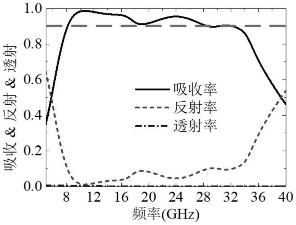
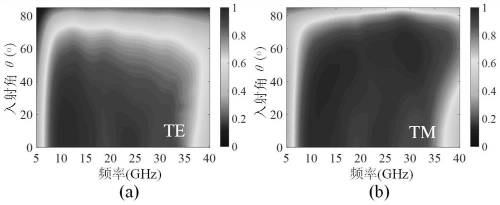
[0042] The properties of the materials prepared in Examples 1-2 are similar, and only the calculation of the absorption characteristics and reflection characteristics is performed on the optically transparent ultra-wideband radar and the infrared double stealth structure in Example 1, as shown in Figure 2-3 As shown, the optically transparent ultra-wideband radar and the infrared double stealth structure in Embodiment 1 can realize broadband wave absorption with a...


PUM

PropertyMeasurementUnit
radiusaaaaaaaaaa
lengthaaaaaaaaaa
thicknessaaaaaaaaaa

Abstract

The invention discloses an optical transparent ultra-wideband radar and infrared double-stealth structure, and relates to the technical field of multi-spectrum stealth, and the stealth structure mainly comprises a low-emissivity infrared stealth layer and an ultra-wideband radar wave-absorbing layer. In order to realize high transmittance of visible light, an optical transparent material transparent conductive film and a transparent dielectric are selected in the overall structural design; the radar wave-absorbing layer adopts a conductive film-medium-conductive film sandwich type wave-absorbing structure; the transparent conductive film is etched into a frequency selective surface by adopting a laser etching process to finish the preparation of the radar and infrared compatible stealth material; the optical transparent ultra-wideband radar and infrared compatible stealth material has high designability, the contradictory problem of optical transparency, radar stealth and infrared stealth can be well solved from the perspective of structural design by adopting a metamaterial technology, and the optical transparent ultra-wideband radar and infrared compatible stealth material has good ultra-wideband radar wave absorption performance, low infrared emissivity and optical transparency.

Description

technical field [0001] The invention relates to the field of multi-spectrum stealth technology, in particular to an optically transparent ultra-wideband radar and infrared double stealth structure. Background technique [0002] With the development of multi-spectrum compound detection technology, the stealth of a single frequency band is far from meeting the stealth requirements of military equipment. Infrared detection and radar detection are currently the most important means of detection, how to be compatible with infrared-radar stealth is the current research hotspot in stealth material technology. Radar stealth requires low reflectivity and high absorptivity, while infrared stealth requires high reflectivity and low absorptivity (low emissivity). It is difficult for traditional materials to have high radar absorption and low infrared emission at the same time. Some researchers proposed to use semiconductor materials zinc oxide (ZnO), indium trioxide (In 2 o 3 ) etc.,...

Claims


Application Information

Patent Timeline
Patent Type & Authority Applications(China)
IPC IPC(8): B32B27/36B32B27/06B32B33/00F41H3/00B23K26/362
CPCB32B27/36B32B27/08B32B27/06B32B33/00F41H3/00B23K26/362
Inventor 王军张雷马华王甲富冯明德赵世鑫随赛屈绍波
Owner AIR FORCE UNIV PLA
Why Eureka
Try Eureka