Metasurface micro-nano structure monolithic full-color waveguide lens and AR display device

A micro-nano structure and metasurface technology, applied in the direction of optical waveguide light guide, optics, instrument, etc., can solve the problems of efficiency fluctuation, small design freedom, low efficiency, etc.

Active Publication Date: 2021-04-09
ZHEJIANG UNIV +2
View PDF13 Cites 8 Cited by
  • Summary
  • Abstract
  • Description
  • Claims
  • Application Information

AI Technical Summary

Problems solved by technology

However, most of the reported diffraction gratings use a single rectangular, triangular or helical tooth design, which contains few variables, has a small degree of design freedom, obtains a small field of view, narrow response spectrum, and low efficiency. Incident light causes large fluctuations in efficiency
In order to achieve full-color display, multi-waveguide lens superposition technology is often required, resulting in the entire imaging system being heavy and poorly wearable

Method used


Image

  • Metasurface micro-nano structure monolithic full-color waveguide lens and AR display device
  • Metasurface micro-nano structure monolithic full-color waveguide lens and AR display device
  • Metasurface micro-nano structure monolithic full-color waveguide lens and AR display device

Examples


Embodiment 1

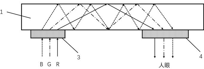
[0033]Such asfigure 1 As shown, a super-surface micro-tape structure monolithic full-color waveguide lens includes a waveguide substrate 1, coupled into a grating 3 and a grating 4; coupled to the grating 3 and the coupling grating 4 are one-dimensional multi-rectangular micro. The structural hyperpot grating is located on the surface of the waveguide substrate, and is distributed at both ends of the waveguide substrate. The coupling of the grating 3 is usually smaller, located in the corner of the lens, and the coupling grating 4 is relatively large, and may occupy the vast majority of lenses.

[0034]Preferably, the refractive index of the waveguide substrate is 1.4-2.2.

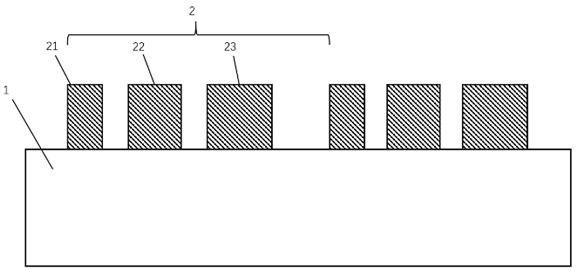
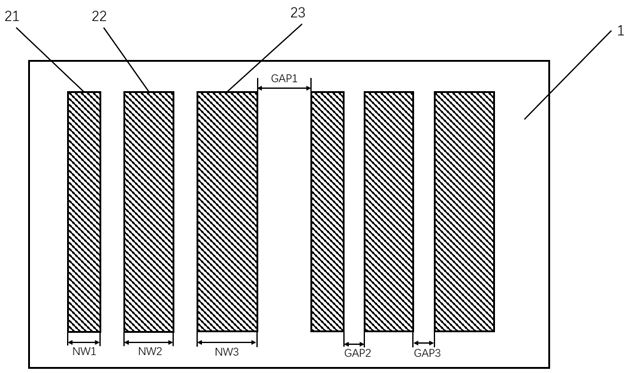
[0035]Such asfigure 2 As shown, one-dimensional multi-rectangular micronidal structure hyperpot grating has a plurality of rectangular micro-tunnel structures in each grating period, the same height of each rectangular micro-structure, but the line width and adjacent rectangular micro-structured structure The spac is ...

Embodiment 2

[0050]This embodiment is further defined based on the first embodiment, except that all components of Example 1, the ultra-surface micro-tank structure single-chip full color waveguide lens also includes the intermediate transfer grating 5 required for two-dimensional expansion;Figure 9As shown, the intermediate transmission grating 5 and the coupling grating 4 are located at the same end of the same waveguide, and in the vertical direction, the intermediate transfer grating 5 is located above the grating 4; wherein the intermediate transfer grating 5 is also a one-dimensional plurality of strips. Rectangular micro-structured hypertrophone grating.

[0051]In this waveguide lens, the grating 3 is coupled to the grating 3, and the blue (B) tri-color optical signal is coupled into the waveguide substrate 1, so that the three-color light is transmitted forward in the form of all reflection; intermediate transmission The grating 5 performs the three-color light transmitted in the waveguide...


PUM

PropertyMeasurementUnit
widthaaaaaaaaaa
refractive indexaaaaaaaaaa

Abstract

The invention discloses a metasurface micro-nano structure monolithic full-color waveguide lens and an AR display device. The metasurface micro-nano structure full-color waveguide lens comprises a waveguide substrate, a coupling-in grating and a coupling-out grating. The coupling-in grating and the coupling-out grating are a plurality of one-dimensional rectangular micro-nano structure metasurface gratings, are located on the surface of the waveguide substrate and are distributed at the two ends of the waveguide substrate; in each period, the coupling-in grating and the coupling-out grating are respectively provided with a plurality of sub-wavelength width rectangular micro-nano metasurface structures. Compared with a conventional grating, the metasurface grating has the resonance effect of different wavelengths, and can have high and balanced first-level transmission diffraction efficiency on red light, green light and blue light at a large incident angle. The lens is large in field angle and high in visual experience, full-color display can be achieved only through a single waveguide lens, and the AR display device adopting the waveguide lens is light in weight and good in wearable performance. Compared with a common grating, the plurality of rectangular micro-nano structure metasurface gratings are more in design variables, flexible in design and easier to process.

Description

Technical field[0001]The present invention relates to the field of transmission grating and the technical field, and more particularly to a super color waveguide lens and an AR display device of a super-surface micro-tube structure.Background technique[0002]Augment Reality; AR) technology is a technique that integrates virtual information with real world. AR eye-catching device represented by AR glasses, passes a series of optical imaging elements to human eye, and its perspective makes real scenes simultaneously. AR glasses wearer can see a real world that superimposes the virtual picture, and the real experience is greatly enhanced. Based on the above features, AR technology has a wide range of application prospects in industrial design, mechanical manufacturing, architecture, education, military and entertainment.[0003]Optical imaging components are used for optical transmission and imaging, and it is the key to the AR glasses. Currently mature optical imaging solutions mainly in...

Claims


Application Information

Patent Timeline
Patent Type & Authority Applications(China)
IPC IPC(8): G02B27/01G02B5/18G02B6/10
CPCG02B27/0172G02B5/1842G02B5/1866G02B5/1814G02B5/1819G02B6/10G02B2027/0178G02B2027/0123G02B2005/1804
Inventor 杨柳古頔阳梁晨晖孙理斌陈杭陈远
Owner ZHEJIANG UNIV
Why Eureka
Try Eureka