Wafer alignment method in photoetching process
A lithography process and wafer technology, applied in photolithography, optics, sustainable manufacturing/processing and other directions on the pattern surface, can solve the problems of scrapped wafers, reduced wafer rotation ratio, increased wafer costs, etc.
- Summary
- Abstract
- Description
- Claims
- Application Information
AI Technical Summary
Problems solved by technology
Method used
Image

Examples
Embodiment Construction
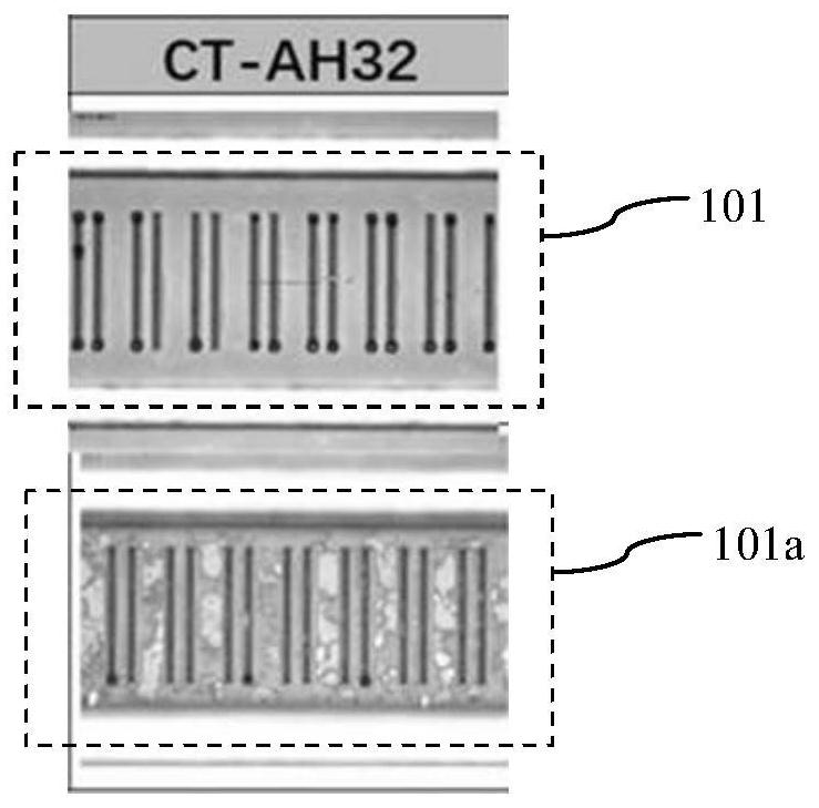
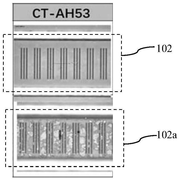
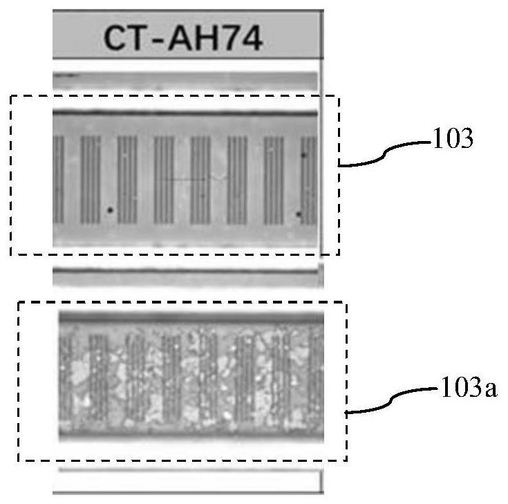
[0052] like image 3 Shown is the flow chart of the wafer alignment method in the photolithography process of the embodiment of the present invention; as Figure 5 Shown is the segmented alignment signal curve in the embodiment of the present invention; in the wafer alignment method in the photolithography process of the embodiment of the present invention, there is an alignment mark on the wafer, and the alignment mark has a grating pattern. The wafer alignment method includes the following steps:
[0053] Step 1: Use the alignment light source to scan the alignment mark in the entire section, and collect the diffracted light signal corresponding to the alignment mark in the entire section to form an alignment signal 1 in the entire section. Figure 5 Only a part of the whole alignment signal 1 is shown in .
[0054] Step 2, segmenting the whole segment of the alignment signal 1 to form each segmented alignment signal. Figure 5 Only three segmented alignment signals are s...
PUM
 Abstract
Description
Claims
Application Information
PatSnap Eureka turns technology decisions into work you can execute. Powered by our Innovation Knowledge Graph, it runs expert workflows across engineering, life sciences, materials and intellectual property. Get your review-ready output in minutes.


