CVD machine table

A machine and plasma technology, applied in gaseous chemical plating, coatings, electrical components, etc., can solve problems such as excessive etching of film layers, difficulty in plasma reaching the bottom of the water tank structure, and affecting product yield.

Pending Publication Date: 2021-04-16
YANGTZE MEMORY TECH CO LTD
View PDF6 Cites 1 Cited by
  • Summary
  • Abstract
  • Description
  • Claims
  • Application Information

AI Technical Summary

Problems solved by technology

[0004] However, due to the continuous updating of the structure of the new generation of 3D NAND, from an open pyramid structure to a closed large tank structure, it is more difficult for the plasma to reach the bottom of the tank structure, and the horizontal component of the plasma will also Further reinforcement of the film on the sidewalls results in a density of the sidewall film that is greater than that of the bottom film
[0005] Then, in the WET process, when the film layer on the top sidewall has just been etched away, the film layer on the bottom has already been over-etched, which seriously affects the product yield.

Method used


Image

  • CVD machine table
  • CVD machine table
  • CVD machine table

Examples


Embodiment Construction

[0040] The following will clearly and completely describe the technical solutions in the embodiments of the present invention with reference to the accompanying drawings in the embodiments of the present invention. Obviously, the described embodiments are only some, not all, embodiments of the present invention. Based on the embodiments of the present invention, all other embodiments obtained by persons of ordinary skill in the art without making creative efforts belong to the protection scope of the present invention.

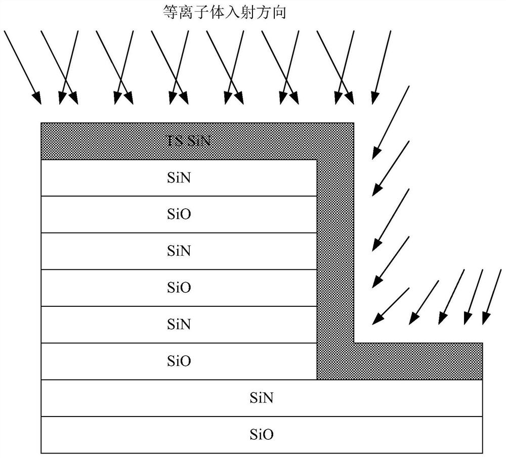
[0041] refer to figure 1 , figure 1 It is a schematic diagram of plasma acting on a wafer to be processed in the prior art. in, figure 1 Only a partial area of ​​the wafer to be processed is shown, and the film layers thereof are illustrated by taking SiN and SiN as examples.

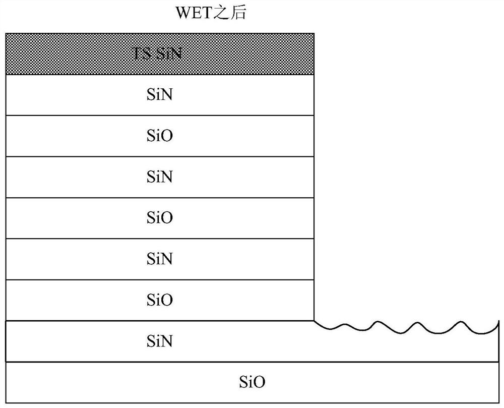
[0042] refer to figure 2 , figure 2 It is a schematic diagram of the film layer morphology of the wafer to be processed after the WET process in the prior art.

[0043] Such as ...


PUM


Abstract

The invention provides a CVD machine table, and the machine table comprises a plasma spray head which is used for spraying plasma; and a plasma adjusting device which is used for changing the direction of the plasma acting on the wafer to be processed into a vertical direction. That is to say, the plasma adjusting device enables the direction of the plasma acting on the to-be-processed wafer to be changed into the vertical direction, so the influence of plasma processing on the side wall can be reduced to a great extent, and the film density of the side wall is enabled to be more loose. Moreover, the plasmas can reach the bottom area more easily, so that the density of the film layers at the top and the bottom is higher, and the density difference of the film layers in the plane area and the side wall area is increased to a great extent; therefore, in the WET process, the film layer on the top side wall is easier to etch, and under the condition that the top side wall is etched, the film layer at the bottom can keep good morphology, so the product yield is improved to a great extent.

Description

technical field [0001] The invention relates to the technical field of semiconductor device design, and more specifically, to a CVD machine. Background technique [0002] In the new generation of 3D NAND front-end SS (Stair case, step treatment) process, after the top oxide is removed, the uppermost layer of the wafer-free stack structure is generally SiN, and then in CVD (Chemical Vapor Deposition, vapor deposition method) magma SiN with different densities is deposited on the machine, and then the sidewall SiN is removed by WET (Wet Etch, wet etching) process. [0003] Among them, SiN is deposited by ALD (Atomic Layer Deposition, atomic layer deposition) process. The ALD process has a strong step coverage ability, and can realize the function of high plasma treatment intensity in the vertical direction, but the plasma treatment effect in the horizontal direction is limited. The deposited density is looser so that the top and bottom film layers are retained while the sidew...

Claims


Application Information

Patent Timeline
Patent Type & Authority Applications(China)
IPC IPC(8): H01L21/67H01L27/11524H01L27/11551H01L27/1157H01L27/11578C23C16/455C23C16/513
Inventor 楚明罗兴安董洪旺涂文骏张高升
Owner YANGTZE MEMORY TECH CO LTD
Why Eureka
Try Eureka