Comparator circuit and RS485 receiver circuit
A comparator circuit and receiver technology, applied in electrical components, differential amplifiers, DC-coupled DC amplifiers, etc., can solve the problems of serial data transmission failure, mismatch of signal voltage rising edge delay and falling edge delay, etc. , to achieve the effect of reducing delay and small delay difference
- Summary
- Abstract
- Description
- Claims
- Application Information
AI Technical Summary
Problems solved by technology
Method used
Image
Examples
Embodiment 1
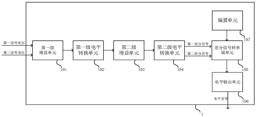
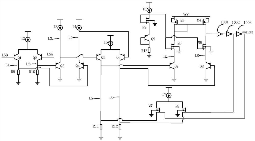
[0044] In high-speed RS485 applications, the transmission signal cycle is very short, and the rising and falling edges of the signal account for a large proportion in the entire cycle. If the rising and falling edge delays do not match, the duty cycle of the signal will change significantly. , in order to convert the A / B signal in RS485 from (-13V, +13V) to (0V, 3V) signal, and at the same time ensure that the first signal voltage LSA and the second signal voltage LSB are in the Within the input common mode range of the comparator, in some requirements, the scaling ratio of the front-stage circuit to the A / B signal is as high as 20 times. At this time, if the input signal A-B is 200mV, the LSA-LSB signal is 10mV, The reduction in signal amplitude rapidly increases the latency of rising and falling edges. If the signal amplitude is asymmetric at this time, for example, the A-B signal is (-200mV, 5V), then the LSA-LSB signal is (-10mV, 250mV), which will cause the delay differen...
Embodiment 2
[0060]This implementation provides an RS485 receiver circuit such as image 3 As shown, the RS485 receiver circuit includes the comparator circuit 1 described in Embodiment 1, the level shift circuit 2 and the output driver circuit 3 . The level shift circuit 2 is connected to the comparator circuit 1 , and the comparator circuit 1 is connected to the output circuit 3 .
[0061] The level shift circuit 2 is used to convert the voltage input by the RS485 bus line A to the first signal voltage LSA, and the level shift circuit 2 is also used to convert the voltage input by the RS485 bus line B to the second signal voltage LSB , the voltage range of the A line input and the B line input is + / -13V.
[0062] The output driving circuit 3 is used for receiving the level signal COMP_OUT output by the comparator circuit 1 and generating and outputting an output signal RO having the same voltage as the level signal. That is, the output signal RO is in the same state as the level signal...
Embodiment 3
[0076] This embodiment provides an integrated circuit, which integrates the RS485 receiver circuit in Embodiment 2.
PUM
 Abstract
Description
Claims
Application Information


