Check patentability & draft patents in minutes with Patsnap Eureka AI!

Gate voltage bootstrap switching circuit applied to ultra-low power consumption analog-to-digital converter

A technology of analog-to-digital converter and grid voltage bootstrap, which is applied in the direction of analog-to-digital converter, analog/digital conversion calibration/test, electronic switch, etc. The effect of small lining offset effect, improved precision and improved linearity

Pending Publication Date: 2021-04-16
GUILIN UNIV OF ELECTRONIC TECH
View PDF0 Cites 1 Cited by
  • Summary
  • Abstract
  • Description
  • Claims
  • Application Information

AI Technical Summary

Problems solved by technology

[0004] The present invention aims to solve the problem that the linearity of the existing grid voltage bootstrap switch circuit is not high, and provides a grid voltage bootstrap switch circuit applied to an ultra-low power consumption analog-to-digital converter

Method used


Image

  • Gate voltage bootstrap switching circuit applied to ultra-low power consumption analog-to-digital converter
  • Gate voltage bootstrap switching circuit applied to ultra-low power consumption analog-to-digital converter
  • Gate voltage bootstrap switching circuit applied to ultra-low power consumption analog-to-digital converter

Examples


Embodiment Construction

[0017] In order to make the object, technical solution and advantages of the present invention clearer, the present invention will be further described in detail below in conjunction with specific examples.

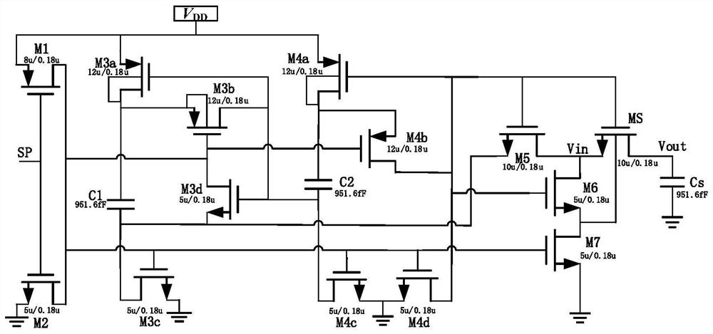
[0018] A gate voltage bootstrap switch circuit for ultra-low power analog-to-digital converters, such as figure 2 As shown, it consists of an input inverter, a first-stage bootstrap circuit, an auxiliary stage bootstrap circuit, a substrate switch and a sampling circuit. The input inverter includes a MOS transistor M1 and a MOS transistor M2. The first stage bootstrap circuit includes MOS transistor M3a, MOS transistor M3b, MOS transistor M3c, MOS transistor M3d and capacitor C1. The auxiliary stage bootstrap circuit includes MOS transistor M4a, MOS transistor M4b, MOS transistor M4c, MOS transistor M4d, MOS transistor M5 and capacitor C2. The substrate switch includes a MOS transistor M6 and a MOS transistor M7. The sampling circuit includes a sampling MOS tube MS an...


PUM


Abstract

The invention discloses a gate voltage bootstrap switching circuit applied to an ultra-low power consumption analog-to-digital converter, which adopts a single-phase clock SP, and sets the gate voltage of a sampling MOS tube MS as Vin+2VDD through a first-stage bootstrap circuit and an auxiliary-stage bootstrap circuit during sampling, so that the gate-source voltage difference of the sampling MOS tube MS is constant as 2VDD in the sampling stage; the conduction resistance of the sampling tube is further reduced, so that the linearity is improved, and the precision of the sampling switch circuit is also improved; and based on the proposed two-stage bootstrap circuit, a sixth NMOS transistor M6 and a seventh NMOS transistor M7 are connected in series to serve as a substrate switch of a sampling MOS transistor MS, and when the bootstrap circuit is in a sampling mode, the grid potential of the sampling MOS transistor MS is kept consistent with the substrate potential, the substrate bias effect of the sampling MOS transistor MS is reduced, and harmonic distortion is reduced.

Description

technical field [0001] The invention relates to the technical field of integrated circuit design, in particular to a gate voltage bootstrap switch circuit applied to an ultra-low power consumption analog-to-digital converter. Background technique [0002] The sampling switch is the front-end circuit of the ultra-low power analog-to-digital converter, which has the function of sampling and holding. The accuracy and linearity it can achieve will affect the system performance of the entire analog-to-digital converter, so the design of the sampling switch circuit is particularly important . The sampling switch in the sampling and holding circuit is divided into three types: a single NMOS tube or PMOS tube, a CMOS transmission gate and a grid voltage bootstrap switching circuit. These three switches have their own advantages. Although the Bootstrap Switch Circuit has a complex structure, it has the advantages of the smallest on-resistance, large input range, and high linearity, ...

Claims


Application Information

Patent Timeline
IPC IPC(8): H03M1/12H03M1/06H03M1/10H03K17/16H03K17/687
Inventor 段吉海周继东韦保林徐卫林韦雪明岳宏卫
Owner GUILIN UNIV OF ELECTRONIC TECH
Features
  • R&D
  • Intellectual Property
  • Life Sciences
  • Materials
  • Tech Scout
  • Unparalleled Data Quality
  • Higher Quality Content
  • 60% Fewer Hallucinations
Learn More