A kind of MEMS inductive pressure sensor and preparation method thereof
A pressure sensor and inductive technology, applied in the field of MEMS, can solve the problems of poor linearity, small temperature drift, and difficult application of MEMS capacitive pressure sensors, and achieve a wide range of applications, small temperature drift, and simple structure Effect
- Summary
- Abstract
- Description
- Claims
- Application Information
AI Technical Summary
Problems solved by technology
Method used
Image
Examples
Embodiment 1
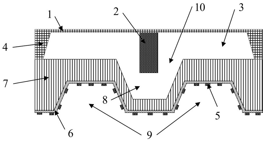
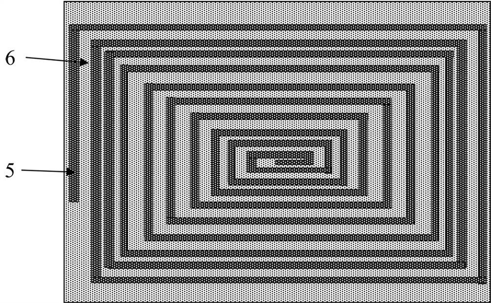
[0035] like Figure 1-2 As shown, the MEMS inductive pressure sensor proposed by the present invention includes a stacked first substrate 4 and a second substrate 7;
[0036] A pressure sensitive film 1 is formed on the upper surface of the first substrate 4; a first groove 3 is formed on the lower surface of the first substrate 4 opposite to the pressure sensitive film 1 by etching;
[0037] A ferromagnetic core 2 is arranged on the lower surface of the pressure sensitive film 1, and the ferromagnetic core 2 is located in the first groove 3;
[0038] The second groove 8 is arranged on the upper surface of the second substrate 7, and forms a vacuum chamber 10 with the first groove 3;
[0039] The third groove 9 is arranged on the lower surface of the second substrate 7 around and spaced apart from the second groove 8;
[0040] The insulating layer 6 is arranged on the lower surface of the second substrate 7;
[0041] The inductor coil layer 5 is provided on the surface of t...
Embodiment 2
[0058] The present invention also proposes a preparation method of a MEMS inductive pressure sensor. Specifically, the preparation method includes the following steps:
[0059] a. Select a 500mm thick N-type (100) single crystal silicon wafer as the first substrate 4, through photolithography and KOH anisotropic wet etching to obtain a first groove 3 with a depth of, for example, 480 μm and a thickness of, for example, 20μm pressure sensitive film 1;
[0060] b. Install a ferromagnetic core 2 on the lower surface of the pressure sensitive film 1 by means of assembly. The ferromagnetic core 2 is, for example, a nickel-iron alloy block, and its dimensions are, for example: length´width´height=200μm´200μm´600μm;
[0061] c. Select a 500mm thick N-type (100) single crystal silicon wafer as the second substrate 7, and perform photolithography and KOH anisotropic wet etching on the upper surface of the second substrate 7 to obtain a depth of, for example, 400 μm, A second groove 8 ...
PUM
| Property | Measurement | Unit |
|---|---|---|
| thickness | aaaaa | aaaaa |
| thickness | aaaaa | aaaaa |
| thickness | aaaaa | aaaaa |
Abstract
Description
Claims
Application Information
 - R&D
- Intellectual Property
- Life Sciences
- Materials
- Tech Scout
- Unparalleled Data Quality
- Higher Quality Content
- 60% Fewer Hallucinations
Browse by: Latest US Patents, China's latest patents, Technical Efficacy Thesaurus, Application Domain, Technology Topic, Popular Technical Reports.
© 2025 PatSnap. All rights reserved.Legal|Privacy policy|Modern Slavery Act Transparency Statement|Sitemap|About US| Contact US: help@patsnap.com


