

Solder resist preparation method and structure for integrating BGA bonding pad on surface of substrate
A substrate surface and pad technology, which is applied in semiconductor/solid-state device manufacturing, semiconductor/solid-state device components, semiconductor devices, etc., can solve problems such as difficult implementation
- Summary
- Abstract
- Description
- Claims
- Application Information
AI Technical Summary
Problems solved by technology
Method used
Image

Examples
Embodiment Construction
[0044] In the following description, specific details such as specific system structures and technologies are presented for the purpose of illustration rather than limitation, so as to thoroughly understand the embodiments of the present invention. It will be apparent, however, to one skilled in the art that the invention may be practiced in other embodiments without these specific details. In other instances, detailed descriptions of well-known systems, devices, circuits, and methods are omitted so as not to obscure the description of the present invention with unnecessary detail.
[0045] In order to illustrate the technical solutions of the present invention, specific examples are used below to illustrate.
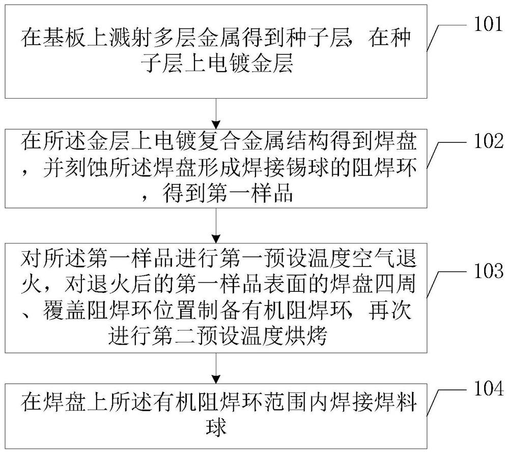
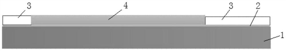
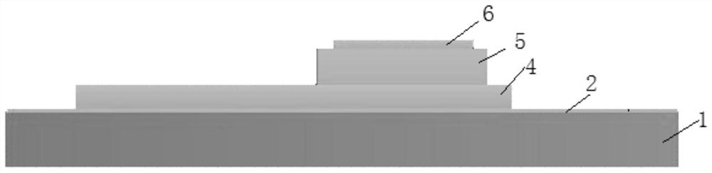
[0046] figure 1 It is a schematic flow diagram of the implementation process of a solder resist preparation method for integrating BGA pads on the surface of the substrate provided by the embodiment of the present invention, which is described in detail as follows.
...
PUM
| Property | Measurement | Unit |
|---|---|---|
| Thickness | aaaaa | aaaaa |
| Thickness | aaaaa | aaaaa |
| Thickness | aaaaa | aaaaa |
Abstract
Description
Claims
Application Information