
Lateral composite grating DFB laser structure and application

A technology of DFB lasers and composite gratings, which is applied to lasers, laser components, semiconductor lasers, etc., can solve the problems of difficult simultaneous realization of high-power lasers, instability of single-mode characteristics, lateral leakage of carriers, etc., and achieve narrow Effects of linewidth and high-power laser output, avoiding secondary epitaxy steps, and improving slope efficiency

Pending Publication Date: 2021-04-20
INST OF SEMICONDUCTORS - CHINESE ACAD OF SCI
View PDF5 Cites 0 Cited by
  • Summary
  • Abstract
  • Description
  • Claims
  • Application Information

AI Technical Summary

Problems solved by technology

[0005] However, the existing side-coupled DFB laser has higher threshold current density and lower slope efficiency than the DFB laser with traditional buried grating. The main reason is that the surface grating is directly fabricated on both sides of the ridge waveguide, and the space is still connected. When electrical injection is performed from the P-side electrode layer, the carriers diffuse through the surface grating regions on both sides of the ridge waveguide, resulting in a large amount of lateral leakage of carriers, thereby increasing the threshold current density of the laser and reducing the slope efficiency.
In addition, most of the currently reported side-coupled DFB lasers are low-order gratings, which have problems such as mode degeneracy and single-mode instability.
Although high-order surface gratings can be prepared by ordinary standard photolithography, such large-size lateral gratings will aggravate the above-mentioned carrier leakage phenomenon, and it is difficult to realize high-power laser

Method used


Image

  • Lateral composite grating DFB laser structure and application
  • Lateral composite grating DFB laser structure and application
  • Lateral composite grating DFB laser structure and application

Examples


Embodiment Construction

[0035] Hereinafter, the present invention will be described in detail with reference to the accompanying drawings and embodiments, in order to assist those skilled in the art to fully understand the objects, features and effects of the present invention. Exemplary embodiments of the present invention are shown in the drawings, but it should be understood that the present application can also be implemented in various other forms and should not be limited by the embodiments described here. Also, in the following description, descriptions of well-known structures and techniques are omitted to avoid unnecessarily obscuring the concept of the present invention. In addition, the various embodiments provided below in the present invention and the technical features in the embodiments can be combined with each other in any manner.

[0036] The terminology used herein is for the purpose of describing particular embodiments only, and is not intended to be limiting of the invention. In...


PUM

PropertyMeasurementUnit
Thicknessaaaaaaaaaa

Abstract

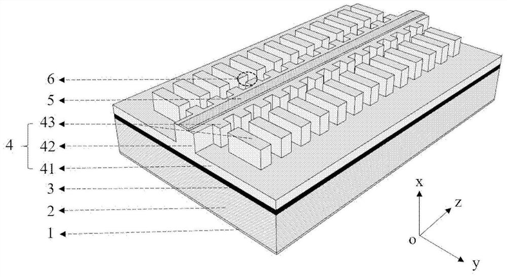
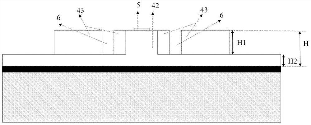
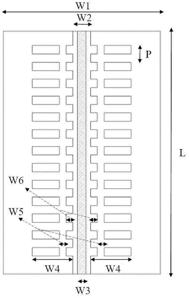
The invention discloses a lateral composite grating DFB laser structure and application. The lateral composite grating DFB laser structure comprises an N-surface electrode layer, the N type waveguide layer arranged on the N-surface electrode layer, an active layer arranged on the N type waveguide layer, a P type waveguide layer arranged on the active layer and a P-surface electrode layer. The P type waveguide layer comprises a non-etched P type waveguide layer, a ridge waveguide and high-order surface lateral gratings, the ridge waveguide and the high-order surface lateral grating are both arranged on the non-etched P type waveguide layer, the high-order surface lateral gratings are arranged on the two sides of the ridge waveguide, and slot areas are arranged at the joint of the high-order surface lateral gratings and the ridge waveguide; and the P-surface electrode layer is disposed on the ridge waveguide. According to the invention, the slot is introduced near the joint of the high-order surface lateral grating and the ridge waveguide for electric isolation, so that carrier leakage caused by the lateral grating during electric injection can be reduced, the threshold current density of the laser is reduced, the slope efficiency is improved, and narrow-linewidth and high-power laser output is realized.

Description

technical field [0001] The invention belongs to the technical field of semiconductor lasers, in particular to a structure and application of a lateral composite grating DFB laser. Background technique [0002] Stable narrow-linewidth and high-power laser sources are widely used in communication, sensing and metrology, and DFB semiconductor lasers are ideal solutions due to their compact size, high efficiency and low manufacturing cost. [0003] For traditional DFB lasers, the grating is etched near the active region, then buried by the upper epitaxial material, and finally the structure continues to grow on the remaining top epitaxial layer. This involves process interruption, exposing the apparent structure to air and other sources of contamination, and creating some defects in the crystal structure close to the active region, affecting the performance of the manufactured device, reducing the yield and reliability of the device. Moreover, secondary epitaxy is a complex, ex...

Claims


Application Information

Patent Timeline
IPC IPC(8): H01S5/12H01S5/20H01S5/22H01S5/042H01S5/065
Inventor 郑婉华徐远博渠红伟王明金王天财刘文振周旭彦
Owner INST OF SEMICONDUCTORS - CHINESE ACAD OF SCI
Learn More