Semiconductor epiaxial structure and light-emitting device thereof

a technology of semiconductors and epiaxial structures, which is applied in semiconductor devices, semiconductor lasers, laser details, etc., can solve the problems of limiting the improvement of device's photoelectric properties, methods still have many urgent problems to be solved, etc., and achieves the reduction of electron ground state level, overall auger recombination, and improved injection of carriers

Inactive Publication Date: 2015-11-26
SOUTH CHINA NORMAL UNIVERSITY
View PDF2 Cites 0 Cited by
  • Summary
  • Abstract
  • Description
  • Claims
  • Application Information

AI Technical Summary

Benefits of technology

[0011]The doping type and / or doping concentration of the band edge shaping layers are different from those of the adjacent layers, which may be non-doping, P-type doping or N-type doping, and the band edge shape of a semiconductor energy band is trimmed through the local built-in electric field formed as a result of adjusting the doping type, doping concentration and / or layer thickness thereof.
[0012]Preferably, the band edge shaping layer trims the band edge shape of the semiconductor energy band of the epiaxial structure through the local built-in electric field formed as a result of adjusting the doping type, doping concentration and / or layer thickness thereof.
[0013]The band edge shaping layer adjusts the position of the electron ground state level of quantum wells in the multi-quantum well active region relative to the quasi fermi level such that the distribution of carrier concentration in the quantum well layer inside the multi-quantum well active region becomes uniform and the overall Auger recombination is decreased.
[0014]When the band edge shaping layer is disposed between the electron injection region and the multi-quantum well active region, the band edge shape of the adjacent energy band structure is trimmed to bend through the local built-in electric field formed as a result of adjusting the doping type, doping concentration and / or layer thickness thereof, the position of the electron ground state level of quantum wells in the multi-quantum well active region relative to the quasi fermi level at the side close to the electron injection region is decreased, and the injection of carriers is improved such that the distribution of carriers in quantum wells of the multi-quantum well active region becomes more uniform, thereby decreasing the overall Auger recombination.
[0015]Preferably, when the band edge shaping layer is disposed between the electron injection region and the multi-quantum well active region, the band edge shaping layer makes the electron ground state level of quantum wells in the multi-quantum well active region to be decreased relative to the quasi fermi level; the farther a quantum well is away from the band edge shaping layer, the less its electron ground state level is decreased relative to the quasi fermi level.
[0016]Preferably, when there are a plurality of band edge shaping layers, they are disposed at both sides of the multi-quantum well active region at the same time, specifically: disposed between the electron injection region and the multi-quantum well active region and disposed together with the potential barrier layer for blocking carriers between the multi-quantum well active region and the hole injection region.

Problems solved by technology

The above methods to improve the internal quantum efficiency of a semiconductor light-emitting device are usually specific to certain devices or structures with very limited applications; in addition, some methods still have many problems in urgent need to be solved.
For example, using a thin film of the wide bandgap material, AlInN, as the barrier of a multi-quantum well active region has low crystal quality as impacted by the current level of epiaxial growth, which limits the improvement of the device's photoelectric properties.

Method used


Image

  • Semiconductor epiaxial structure and light-emitting device thereof
  • Semiconductor epiaxial structure and light-emitting device thereof
  • Semiconductor epiaxial structure and light-emitting device thereof

Examples


example i

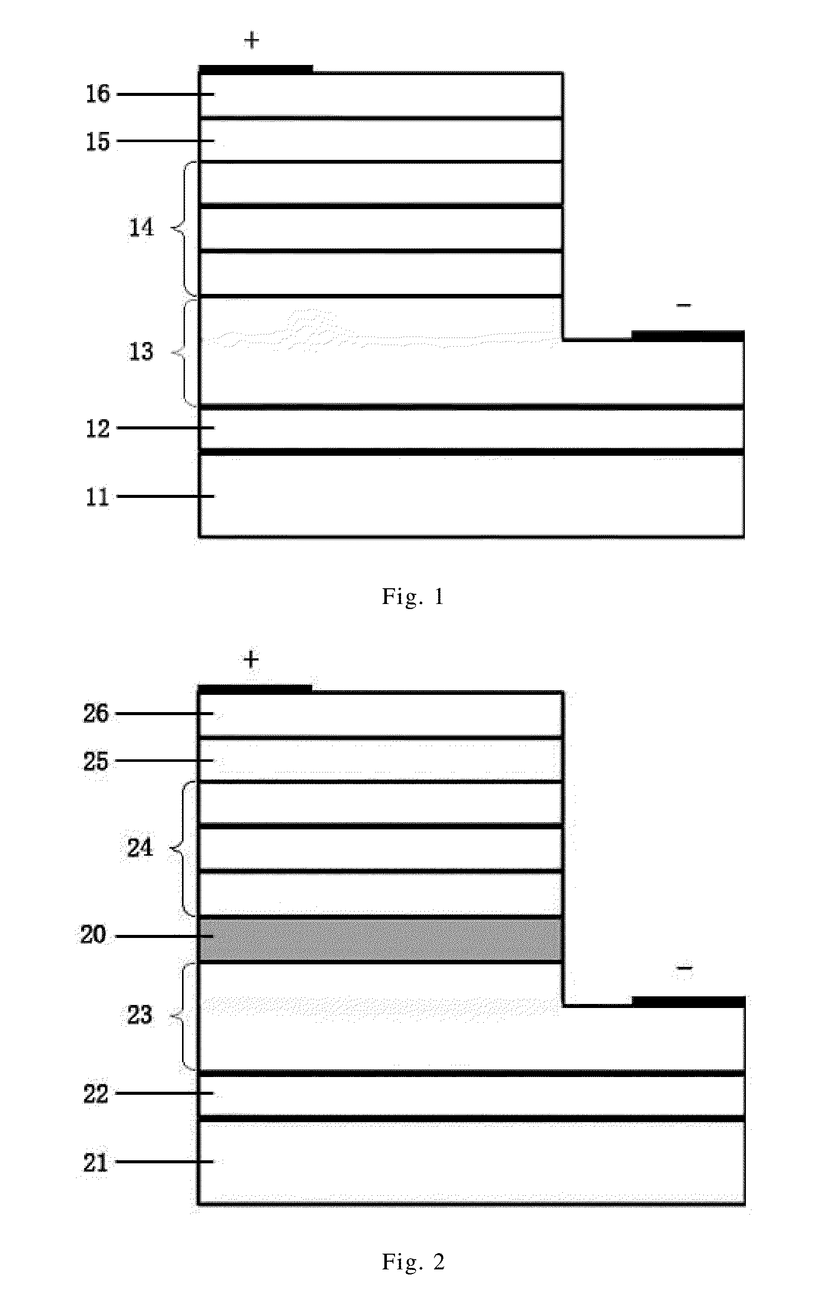
[0067]As shown in FIG. 2, the epiaxial structure of the light-emitting diode comprises sequentially from bottom up: a substrate layer 21, a nucleation layer 22, a N-type electron injection layer 23, a band edge shaping layer 20, a multi-quantum well active region 24, an electron blocking layer 25 and a P-type hole injection layer 26. Relative to the prior art, the band edge shaping layer 20 is introduced between the N-type electron injection layer 23 and the multi-quantum well active region 24.

[0068]The thickness of the band edge shaping layer 20 is 1 nm˜100 nm, the material is P-type doped GaN, the doping concentration is 1×1017 cm−3 ˜5×1018 cm−3, and the dopant is Cp2Mg.

[0069]In this example, one most preferred selection is: the thickness of the band edge shaping layer 20 is 20 nm and the doping concentration is 5×1017 cm−3. The inventors have shown through actual tests that when it is the n-type doping or un-doping, and when the thickness is not 20 nm, the result is still optimiz...

example ii

[0074]As shown in FIG. 8, the epiaxial structure of the light-emitting diode comprises sequentially from bottom up: a substrate layer 31, a nucleation layer 32, a N-type electron injection layer 33, a multi-quantum well active region 34, a band edge shaping layer 30, an electron blocking layer 35 and a P-type hole injection layer 36. Relative to the prior art, the band edge shaping layer 30 is introduced between the electron blocking layer 35 and the multi-quantum well active region 34.

[0075]The thickness of the band edge shaping layer 30 is 1 nm˜300 nm, the material is P-type doped GaN, the doping concentration is 1×1017 cm−3 ˜5×1018 cm−3, and the dopant is Cp2Mg.

[0076]In this example, one most preferred selection is: the thickness of the band edge shaping layer 30 is 50 nm and the doping concentration is 3×1017 cm−3. The inventors have shown through actual tests that when it is the n-type doping or un-doping, and when the thickness is not 50 nm, the result is still optimized relat...

example iii

[0081]As shown in FIG. 12, the epiaxial structure of the light-emitting diode comprises sequentially from bottom up: a substrate layer 41, a nucleation layer 42, a N-type electron injection layer 43, a second band edge shaping layer 40b, a multi-quantum well active region 44, a first band edge shaping layer 40a, an electron blocking layer 45 and a P-type hole injection layer 46. Relative to the prior art, the second band edge shaping layer 40b is introduced between the N-type electron injection layer 43 and the multi-quantum well active region 44, and the first band edge shaping layer 40a is introduced between the electron blocking layer 45 and the multi-quantum well active region 44.

[0082]The thickness of the first band edge shaping layer 40a is 1 nm˜300 nm, the material is P-type doped GaN, the doping concentration is 1×1017 cm−3 ˜5×1018 cm−3, and the dopant is Cp2Mg. In this example, a preferred selection is that the thickness of the first band edge shaping layer 40a is 50 nm and...


PUM


Abstract

The present invention discloses an epiaxial structure for semiconductor light-emitting device, comprising an electron injection region, a hole injection region, a multi-quantum well active region, a potential barrier layer for blocking carriers, and one or more band edge shaping layers. The doping type and/or doping concentration of said band edge shaping layers are different from those of the adjacent layers. It may trim the band edge shape of the semiconductor energy band through the local built-in electric field formed as a result of adjusting the doping type, doping concentration and/or layer thickness thereof, such that the carriers in the multi-quantum well active region are distributed uniformly, the overall Auger recombination is decreased, and the effective potential barrier height of the potential barrier layer for blocking carriers is increased to reduce the drain current formed by carriers overflowing out of the multi-quantum well active region, thereby improving internal quantum efficiency. The present invention further discloses a semiconductor light-emitting device that employs said epiaxial structure, which similarly achieves the effects of reduced Auger recombination and/or decreased drain current through the trimming of the band edge shape of the energy band structure by the local built-in electric field, thereby improving internal quantum efficiency of the device.

Description

FIELD OF THE INVENTION[0001]The present invention relates to the technical field of semiconductor light-emitting devices and specifically to an epiaxial structure that uses local built-in electric field to trim the energy band structure so as to improve internal quantum efficiency. The present invention further relates to semiconductor light-emitting devices that employ said epiaxial structure.DESCRIPTION OF THE PRIOR ART[0002]Semiconductor light-emitting devices typically include semiconductor laser diodes (LD) and semiconductor light-emitting diode (LED). A carrier injection region includes electron injection region and hole injection region. A multi-quantum well active region is a periodic structure formed by alternately stacked quantum well layers and barrier layers, and electrons and holes are recombined in the quantum well layer to produce photons. A potential barrier layer for blocking carriers is disposed between a multi-quantum well active region and a carrier injection reg...

Claims


Application Information

Patent Timeline
Patent Type & Authority Applications(United States)
IPC IPC(8): H01L33/06H01S5/343H01S5/042H01L33/14
CPCH01L33/06H01L33/14H01S5/0421H01S5/34333H01S5/34346H01L33/145H01S5/2009H01S5/3054H01S2301/17
Inventor MEI, TINGWANG, NAIYINLI, HAOWAN, LEI
Owner SOUTH CHINA NORMAL UNIVERSITY
Why Eureka
Try Eureka