

Novel circuit board ink windowing method
A circuit board and ink technology, which is applied in the secondary processing of printed circuits, coating non-metallic protective layers, etc., can solve problems such as inability to guarantee ink bridges
- Summary
- Abstract
- Description
- Claims
- Application Information
AI Technical Summary
Problems solved by technology
Method used
Image

Examples
Embodiment Construction
[0022] The following will clearly and completely describe the technical solutions in the embodiments of the present invention with reference to the drawings in the embodiments of the present invention.
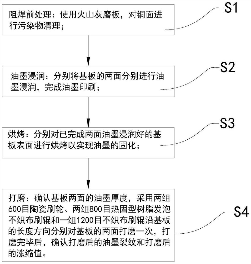
[0023] Such as figure 1 As shown, one embodiment of the present invention discloses a novel circuit board ink window opening method, comprising the following steps:
[0024] S1: Pre-treatment of solder resistance: make the circuit board lamp face down and enter the board along the length direction, use volcanic ash grinding plate, the grinding plate parameter is 2.5m / min; the grinding mark control is 6mm; the spray pressure is 1.2 / bar to remove the pollutants on the board surface And copper surface oxidation, synchronously roughened copper surface enhances ink adhesion;
[0025] S2: Ink infiltration: Ink infiltration is performed on both sides of the substrate respectively to complete ink printing;
[0026] S3: Baking: Baking the surface of the substrate that has been infilt...
PUM
 Abstract
Description
Claims
Application Information