Thermoelectric coupling modeling method of power semiconductor chip cell

A power semiconductor and thermoelectric coupling technology, applied in CAD numerical modeling, electrical digital data processing, instruments, etc., can solve the problem of accurate characterization of chip electrical characteristics, prediction of chip electrical temperature field accuracy disadvantages, and complex application environment of power semiconductor chips And other issues

Active Publication Date: 2021-04-23
ZHEJIANG UNIV
View PDF12 Cites 2 Cited by
  • Summary
  • Abstract
  • Description
  • Claims
  • Application Information

AI Technical Summary

Problems solved by technology

However, this type of finite element simulation software adopts Ohm's law to solve the thermoelectric coupling effect, that is, the object of solution is required to be pure resistance characteristics, and the electrical characteristics of power semiconductor chips are essentially different from pure resistance, and the chip conductivity is also greatly different from that of silicon. Material conductivity, which limits the ability of finite element software to solve problems that take into account the electrical properties of semiconductor chips
In addition, under actual application conditions, the application environment of power semiconductor chips is complex, and the external working conditions such as voltage and current are in a state of drastic changes, and the finite element commercial software cannot accurately characterize the electrical characteristics of the chip under the continuous change of current, and then predict the chip electrical characteristics. There is a great disadvantage in the accuracy of the electric temperature field

Method used


Image

  • Thermoelectric coupling modeling method of power semiconductor chip cell
  • Thermoelectric coupling modeling method of power semiconductor chip cell
  • Thermoelectric coupling modeling method of power semiconductor chip cell

Examples


Embodiment Construction

[0056] In order to explain the present invention in more detail, the present invention will be further described in detail below in conjunction with the accompanying drawings, taking the SEMiKron power semiconductor module SEMiX603GB12E4p as an example.

[0057] The thermoelectric coupling modeling method of the power semiconductor chip cell proposed by the present invention, the specific steps include:

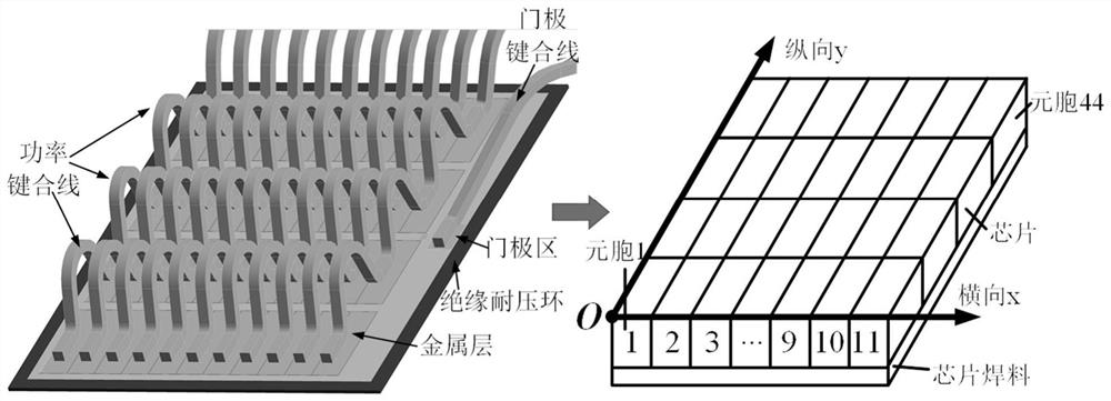
[0058] S1. Based on the chip metal layer and bonding wire layout characteristics, the power semiconductor chip is divided into a multi-cell structure;

[0059] S2. Extract chip lumped parameters, and use the least squares algorithm to establish a voltage-current-temperature three-dimensional model of the power semiconductor chip;

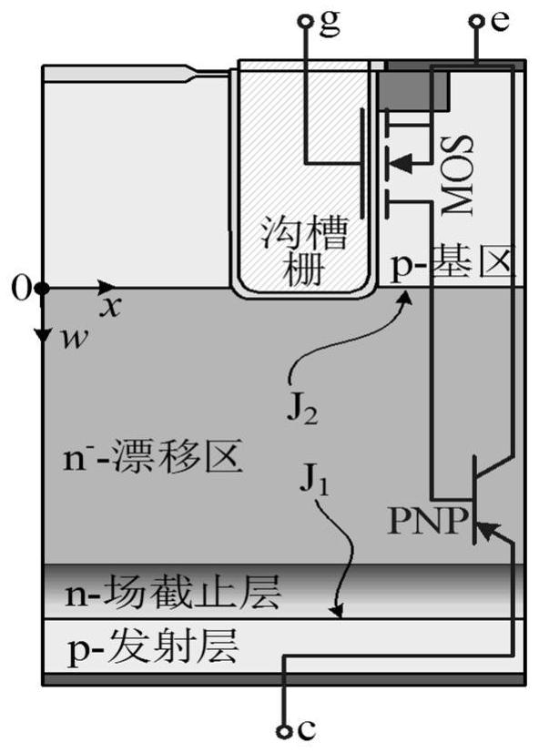
[0060] S3. According to the characteristics of the multi-cell parallel circuit, the chip lumped parameters are converted into cell distribution parameters, and the voltage-current-temperature three-dimensional model of the power semiconductor cell ...


PUM

PropertyMeasurementUnit
thicknessaaaaaaaaaa

Abstract

The invention discloses a thermoelectric coupling modeling method of a power semiconductor chip cell. The method comprises the following steps: S1, dividing a power semiconductor chip into a multi-cell structure; s2, extracting a voltage-current-temperature three-dimensional model of the chip; s3, extracting a voltage-current-temperature three-dimensional model of the cell; s4, solving a cellular current distribution proportion and corresponding loss under any temperature distribution; s5, superposing the temperature rise generated by each cell to obtain the overall temperature gradient of the chip; s6, repeating the steps S4 and S5 until the temperature gradient deviation is converged; and S7, extracting chip surface temperature peak values under different working conditions, and calculating corresponding power module thermal resistance. According to the method, a chip lumped Fourier series analytical thermal model is combined with a multi-cell distributed electrical model, so that thermoelectric coupling modeling and calculation of power semiconductor chip cells are achieved. Besides, the method has the advantages of small required calculation amount, short solving time and no convergence problem, and is particularly suitable for online prediction of the temperature of the power semiconductor chip.

Description

technical field [0001] The invention belongs to the field of power electronic devices, and in particular relates to a thermoelectric coupling modeling method of power semiconductor chip cells. Background technique [0002] Power modules are widely used in new energy vehicle powertrain systems. The trend of high power density and high integration intensifies the temperature gradient on the chip surface, and the electrical parameters of the cells have a temperature change effect, which leads to the uneven distribution of current density on the chip. Due to the over-current operation of semiconductor chips under extreme working conditions such as low-speed high-torque, heavy-duty stator stalls, and acceleration during start-up, the uneven distribution of cell current is more serious, and the formation mechanism of the on-chip temperature field is still unclear. to hidden dangers. Therefore, it is particularly urgent to model and analyze the electrical temperature field on the...

Claims


Application Information

Patent Timeline
Patent Type & Authority Applications(China)
IPC IPC(8): G06F30/23G06F30/398G06F17/13G06F17/14G06F111/10G06F119/08
CPCG06F30/23G06F30/398G06F17/13G06F17/14G06F2111/10G06F2119/08
Inventor 李武华陈宇吴强周宇罗皓泽何湘宁
Owner ZHEJIANG UNIV
Why Eureka
Try Eureka