Method for shortening sensing delay, multiplexer and nonvolatile memory read circuit
A read circuit and non-volatile technology, applied in the field of delay period circuits, multiplexers and non-volatile memory read circuits, can solve the problem of increasing the inherent resistance of address lines and sense amplifiers, reducing address line and sense amplifier gain issues
- Summary
- Abstract
- Description
- Claims
- Application Information
AI Technical Summary
Problems solved by technology
Method used
Image
Examples
Embodiment Construction
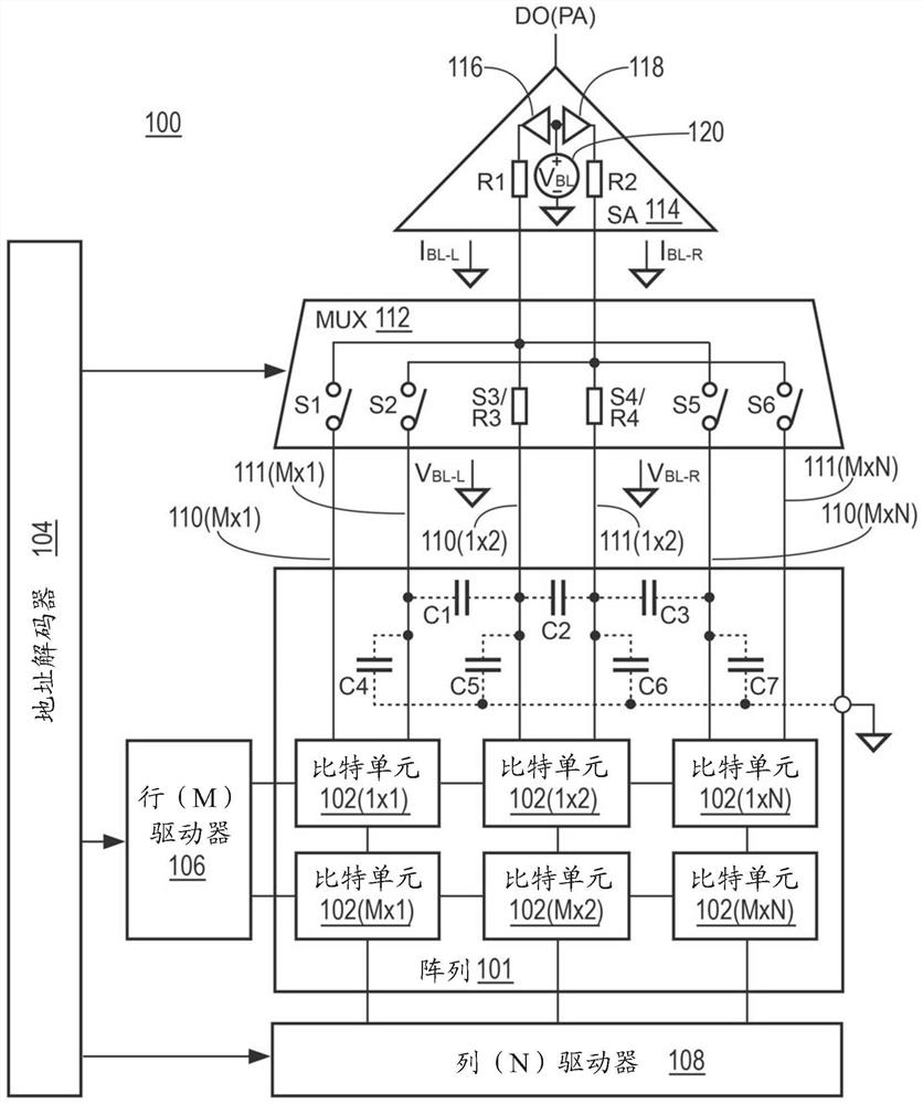
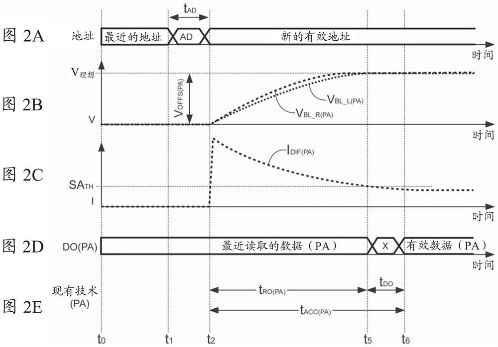
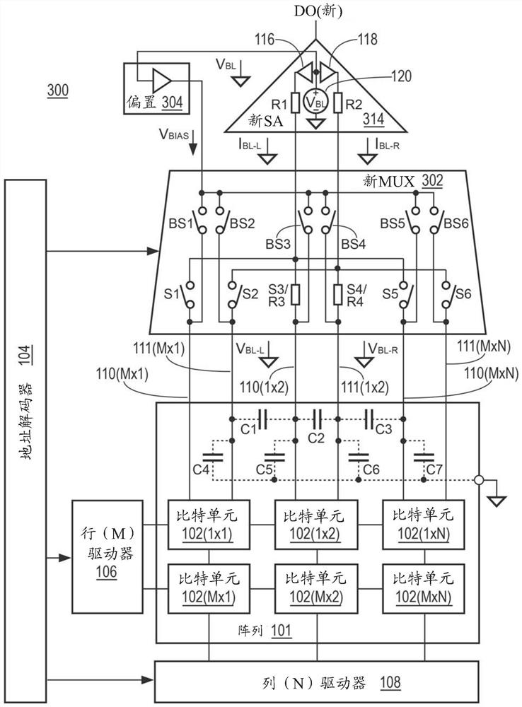
[0033] Various embodiments described herein relate to circuits and methods configured to shorten a delay period associated with reading a selected NVM cell. Such as figure 1 As shown, a prior art non-volatile memory (NVM) read circuit 100 typically operates on an array 100 of memory cells (herein "bit cells") 102 . Bit cells 102 are typically arranged in rows and columns with "M" rows and "N" columns (where M and N are integers), for example, bit cells 102(1x1), 102(1x2) through 102(MxN) . Any number of rows and columns can be used for array 101, and other formats can also be used. Each bit cell can be selected individually by using address decoder 104 , row M driver 106 and column N driver 108 . Each bit cell is typically coupled via a pair of bit lines 110 (MxN) and 111 (MxN) to a multiplexer ("MUX") 112 providing a respective read switch S1 to S6. When the read switch is selected by MUX 112, the read switch is closed and the data stored on the selected bit cell ("bit ce...
PUM
 Abstract
Description
Claims
Application Information
 - R&D Engineer
- R&D Manager
- IP Professional
- Industry Leading Data Capabilities
- Powerful AI technology
- Patent DNA Extraction
Browse by: Latest US Patents, China's latest patents, Technical Efficacy Thesaurus, Application Domain, Technology Topic, Popular Technical Reports.
© 2024 PatSnap. All rights reserved.Legal|Privacy policy|Modern Slavery Act Transparency Statement|Sitemap|About US| Contact US: help@patsnap.com


